Biomedical Engineering Reference
In-Depth Information
Support
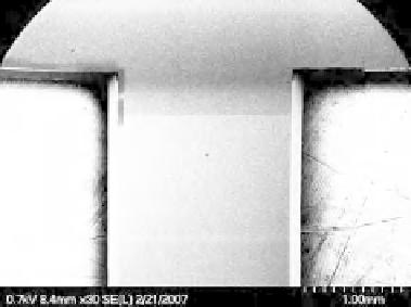
{111} Plane
Beam
Figure 4.31
A micromachined beam and a support. (The (100) plane, which is parallel to the
paper is shown. The
{
111
}
planes which make two sides of the beam are also illustrated)
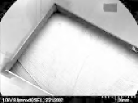
Beam
Beam
Figure 4.32
The void space between two adjacent beams
Due to the presence of silicon during TMAH etching, the existing oxide layer at the
edges showed some irregularities. To achieve a uniform surface, it was decided to remove
all existing oxide layers and repeat the oxidation step at the end. In this way a uniform
and smooth surface of oxide layer was grown on the wafers.
To remove the oxide layer, the samples were treated as stated in Section 4.2.3.6, and then
the process of wet oxidation, as explained in Section 4.2.3.4, was repeated. Figures 4.31
and 4.32 show an SEM (scanning electron micrograph) of the fabricated parts.
Figure 4.31 shows the void between two beams while Figure 4.32 illustrates a beam and
its support.
The
{
111
}
planes which are at an angle of 54.7
◦
with the (100) plane can also be seen
in Figure 4.31.
4.2.4 Sensor Assembly
Using the silicon micro-machined parts and PVDF films, a complete sensing module was
assembled. As mentioned earlier, five PVDF films were used, two as supports and the
other three for the beams. A 28 μm thick, uniaxial, and metalized PVDF film was used