Biomedical Engineering Reference
In-Depth Information
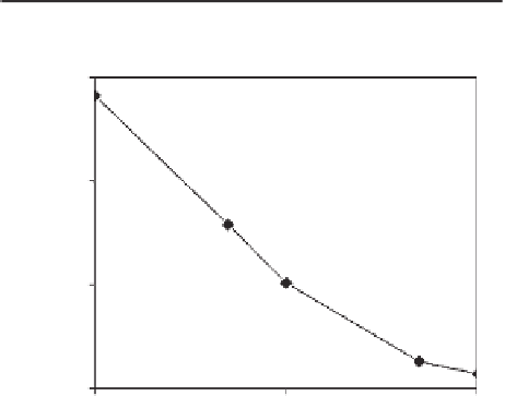
Table 4.1
The maximum beam deflection at the center,
Y
max
, the corresponding stress in the
x
-direction,
σ
x
,
and the output voltage of the middle PVDF film,
V
mid
when the Young's modulus of the contact object,
E
obj
is
varied between 0.01 and 1 MPa
E
obj
(MPa)
Y
max
(
μ
m)
σ
x
(MPa)
V
mid
(mV)
0.01
−
20.4
78.6
170
0.05
−
11.2
39.6
95.2
0.1
−
7.2
22.8
61.2
−
0.5
1.8
4.6
15.3
−
1
1.0
2.4
8.5
180
120
60
0
0.01
0.1
1
Young's modulus (MPa)
Figure 4.24
The output of the middle PVDF film at constant pressure 111 kPa when the Young's
modulus of the contact object is varied between 0.01 and 1 MPa
dimensions and attached in their positions. This section describes the different steps used
in the manufacturing of the sensor.
Both silicon parts of the sensor were micromachined using anisotropic wet etching.
In order to increase the sensitivity of the sensor, the thickness of the beams was consid-
ered to be less than 200 μm. As conventional 500 μm silicon wafer would require an
extra 300 μm back etching, a 180 μm thick, 4 inch (100 mm) silicon wafer was used for
the fabrication. Several designs with different numbers of beams were considered. The
bottom part, however, was the same for all designs. Figure 4.25 shows the steps in the
fabrication procedure. A brief explanation of each step of silicon fabrication is schemati-
cally shown in Figure 4.26. For simplicity, the cross section of one beam only is shown.
The same procedure was used for both silicon parts, however, only the tetramethylam-
monium hydroxide (TMAH) etching (step 9) time was different for bottom and top parts.
More explanation on each step is given below. As the first step, the silicon wafer was
diced into the required dimensions (18
×
18 mm).