Biomedical Engineering Reference
In-Depth Information
For many biomedical applications, there is a need for
porous implant materials. They can be used for artificial
blood vessels, artificial skin, drug delivery, bone and car-
tilage reconstruction, periodontal repair, and tissue engi-
neering (
Lanza
et al.
, 1997
). For each application, the
porous materials have to fulfil a number of specific re-
quirements. For example, for bone ingrowth the optimum
pore size is in the range of 75-250
m
m(
Pilliar, 1987
). On
the other hand, for ingrowth of fibrocartilagenous tissue
the recommended pore size ranges from 200 to 300
m
m
(
Elema
et al.
, 1990
). Besides pore size, other parameters
play a role, such as compressibility, pore interconnectivity,
pore interconnection throat size, and possibly degradi-
bility of the porous material (de
Groot
et al.
, 1990
).
Although porosity can also be discerned as a different
class of surface irregularity, the following sections will
consider porosity as microtexture, much like other sur-
face features. This choice is based on the many reports
that emphasize the importance of this type of surface
morphology for cell and tissue response.
lithographically defined PR pattern is transferred into the
underlying material by etching. This etching can be
performed under wet or dry conditions. In the first sit-
uation, materials are placed in chemicals. Etch direction
is along the crystal planes of the material. In the second
situation, dry etching is performed using directed ions
from a plasma or ion beam as etchants. This technique of
physical etching allows a higher resolution than the wet
technique. It is also applicable in noncrystalline materials
because of the etch directionality without using crystal
orientation. Finally, after the etching process, the
remaining resist is removed. If a substrate is formed with
microgrooves, the dimensions of the texture are usually
described in pitch (or spacing), ridge width, and groove
width (
von Recum and van Kooten, 1995
).
Plasma and ion etching techniques can be used to
create micropatterns in a wide variety of biopolymers.
The micropatterns can be prepared directly in the poly-
mer surface or transferred into the polymer surface via
solvent-casting or injection-molding methods, whereby
a micropatterned silicon wafer is used as a template
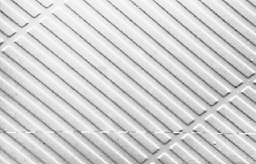
(
Fig. 3.2.15-1
).
Preparation of surface
microtexture
Liga
For the production of microtextured implant surfaces,
numerous techniques are available ranging from simple
manual scratching to more controlled fabrication
methods. For example, from semiconductor technology,
photolithographic techniques used in conjunction with
reactive plasma and ion-etching, LIGA and electro-
forming, have become available. Deep reactive ion etching
(DRIE) enhances the depth of surface etched features and
gives parallel sidewallsdit is especially well suited for
microelectromechanical systems (MEMS) fabrication.
m
CP allows patterns to be transferred to biomaterial sur-
faces by a rubber stamp. Because these techniques are
relatively fast and cheap, and also allow the texturing of
surfaces of reasonable size, they appear to be promising for
biomedical research and applications. Other methods
that offer the ability to texture and pattern surfaces in-
clude UV laser machining, electron-beam etching, and
ion-beam etching.
Another technology suitable for creating surface micro-
textures is the so-called LIGA process (
Rogner
et al.
,
1992
). LIGA refers to the German ''Lithographie,
Galvanoformung, Abformung'' (lithography, electro-
plating, molding). The LIGA technique differs com-
pletely from that described in the preceding section,
since it is not based on etching. In the LIGA process
a thick X-ray-resistant layer is exposed to synchrotron
radiation using a special X-ray mask membrane. Sub-
sequently, the exposed layer is developed, which results
in the desired resist structure. Then, metal is deposited
Reactive plasma and ion etching
For this method the material, usually silicon, is first
cleaned and dried with filtered air (
den Braber
et al.
,
1998a
; Hoch
et al.
, 1996;
Jansen
et al.,
1996
). Then it is
coated with a primer and PR material. Photolithography
is used to create a micropattern in the PR layer. Masks
with predetermined dimensions are exposed with either
UV light or electron beams depending on the size of the
required surface configuration. Subsequently, the ex-
posed resist is developed and rinsed off. Finally, this
Fig. 3.2.15-1 Scanning electron micrograph of a micropatterned
silicon wafer, which can be used as a template in a solvent-casting
replication process.