Biomedical Engineering Reference
In-Depth Information
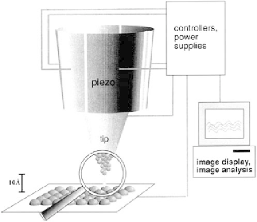
the change in current with distance traveled along the
plane of the surface is directly recorded. A schematic
diagram of a scanning tunneling microscope is presented
in
Fig. 3.1.4-13
. Two STM scanning modes are illustrated
in
Fig. 3.1.4-14
.
The STM measures electrical current and therefore is
well suited for conductive and semiconductive surfaces.
However, biomolecules (even proteins) on conductive
substrates appear amenable to imaging. It must be re-
membered that STM does not ''see'' atoms, but monitors
electron density. The conductive and imaging mechanism
for proteins is not well understood. Still,
Fig. 3.1.4-15
suggests that valuable images of biomolecules on con-
ductive surfaces can be obtained.
The AFM uses a similar piezo drive mechanism. How-
ever, instead of recording tunneling current, the deflection
of a tip mounted on a flexible cantilever arm due to van der
Waals and electrostatic repulsion and attraction between an
atom at the tip and an atom on the surface is measured.
Atomic-scale measurements of cantilever armmovements
can be made by reflecting a laser beam off a mirror on the
cantilever arm (an optical lever). A one-atom deflection of
the cantilever arm can easily be magnified by monitoring
the position of the laser reflection on a spatially resolved
photosensitive detector. Other principles are also used to
measure the deflection of the tip. These include capaci-
tance measurements and interferometry. A diagram of
a typical AFM is presented in
Fig. 3.1.4-16
.
Tips are important in AFM as the spatial resolution of
the method is significantly associated with tip terminal
diameter and shape. Tips are made frommicrolithographi-
cally fabricated silicon or silicon nitride. Also carbon
whiskers, nanotubes, and a variety of nanospherical parti-
cles have been mounted on AFM tips to increase their
sharpness or improve the ability to precisely define tip
geometry. Tips are also surface-modified to alter the
strength and types of interactions with surfaces (static
SIMS can be used to image these surface modifications).
Finally, cantilevers are sold in a range of stiffnesses so the
analysis modes can be tuned to needs of the sample and
the type of data being acquired. The forces associated with
the interaction of an AFM tip with a surface as it ap-
proaches and is retracted are illustrated in
Fig. 3.1.4-16
.
Since force is being measured and Hooke's law applies to
the deformation of an elastic cantilever, the AFM can be
used to quantify the forces between surface and tip. An
exciting application of AFM is to measure the strength of
interaction between two biomolecules (for example, biotin
and streptavidin; see
Chilkoti
et al.
,1995
).
AFM instruments are commonly applied to surface
problems using one of two modes, contact mode and tap-
ping mode. In contact mode, the tip is in contact with the
surface (or at least the electron clouds of tip and surface
essentially overlap). The pressures resulting from the force
of the cantilever delivered through the extremely small
Fig. 3.1.4-13 Schematic diagram illustrating the principle of the
STM
d
a tip terminating in a single atom permits localized quantum
tunneling current from surface features (or atoms) to tip. This
tunneling current can be spatially reconstructed to
form an image.
The STM was invented in 1981 and led to a Nobel
Prize for Binnig and Rohrer in 1986. The STM uses
quantum tunneling to generate an atom-scale electron
density image of a surface. A metal tip terminating in
a single atom is brought within 5-10
˚
of an electrically
conducting surface. At these distances, the electron
cloud of the atom at the ''tip of the tip'' will significantly
overlap the electron cloud of an atom on the surface. If
a potential is applied between the tip and the surface, an
electron tunneling current will be established whose
magnitude,
J
, follows the proportionality:
J
f
e
ðAk
0
SÞ
where
A
is a constant,
k
0
is an average inverse decay
length (related to the electron affinity of the metals), and
S
is the separation distance in angstrom units. For most
metals, a 1
˚
change in the distance of the tip from the
surface results in an order of magnitude change in tun-
neling current. Even though this current is small, it can be
measured with good accuracy.
To image a surface, this quantum tunneling current is
used in one of two ways. In constant current mode, a pi-
ezoelectric driver scans a tip over a surface. When the tip
approaches an atom protruding above the plane of the
surface, the current rapidly increases, and a feedback
circuit moves the tip up to keep the current constant.
Then, a plot is made of the tip height required to maintain
constant current versus distance along the plane. In con-
stant height mode, the tip is moved over the surface and