Biomedical Engineering Reference
In-Depth Information
spectral interpretation. A more complete introduction to
the concepts behind static SIMS spectral interpretation
can be found in
Van Vaeck
et al.
, (1999)
or in standard
texts on mass spectrometry.
Magnetically or electrostatically focusing the primary
ion beam permits the SIMS technique to have high
spatial resolution in the
x,y
plane. In fact, SIMS analysis
can be performed in surface regions of 10 nm diameter or
smaller. For static SIMS analysis, less than 10% of the
atoms in any area are sampled. Thus, as the spot size gets
smaller, the challenge to achieve high analytical sensi-
tivity increases sharply. Still, static SIMS measurements
have been performed in areas as small as 40 nm. Newly
developed cluster ion sources (for example, using gold
molecular clusters, Au
3
,orC
60
as the impacting primary
particles) show high secondary ion yields and relatively
low surface damage. These may improve spatial resolu-
tion and also permit depth profiling of organic surfaces by
sputtering down into a surface while monitoring sec-
ondary ion emission as a function of time.
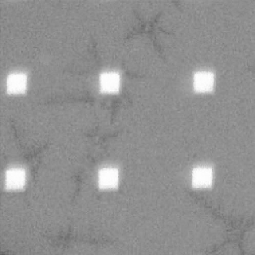
If the focused primary ion beam is rastered over the
surface and the
x,y
position of the beam correlated with
the signal emitted from a given spot, the SIMS data can
be converted into an elemental image. Patterning and
spatial control of chemistry is becoming increasingly
important in biomaterials surface design. For example,
microcontact printing allows patterned chemistry to be
transferred to surfaces at the micron level using a rela-
tively simple rubber stamp. Imaging SIMS is well suited
to studying and monitoring such spatially defined
chemistry. An example is presented in
Fig. 3.1.4-11
.
Imaging SIMS is also valuable for observing defects in
thin films (pinholes), analyzing the chemistry of fine
particulates or assessing causes of implant failure.
Fig. 3.1.4-11 Static SIMS image of protein islands on a
poly(ethylene oxide) background. (For details, see Veiseh, M.,
Wickes, B. T., Castner, D. G., Zhang, M., ''Guided cell
patterning by surface molecular engineering.'' In press.)
the shallow penetration depth of the low-energy sec-
ondary electrons produced by the primary electron beam,
only secondary electrons generated near the surface can
escape from the bulk and be detected (this is analogous to
the surface sensitivity described in
Fig. 3.1.4-7
). Conse-
quently, SEM is a surface analysis method.
Nonconductive materials observed in the SEM are
typically coated with a thin, electrically grounded layer of
metal to minimize negative charge accumulation from the
electron beam. However, this metal layer is always so
thick (
>
200
˚
) that the electrons emitted from the
sample beneath cannot penetrate. Therefore, in SEM
analysis of nonconductors, the surface of themetal coating
is, in effect, being monitored. If the metal coat is truly
conformal, a good representation of the surface geometry
will be conveyed. However, the specimen surface chem-
istry no longer influences secondary electron emission.
Also, at very high magnifications, the texture of the metal
coat and not the surface may be under observation.
SEM, in spite of these limitations in providing true
surface information, is an important corroborative method
to use in conjunction with other surface analysis methods.
Surface roughness and texture can have a profound in-
fluence on data from ESCA, SIMS, and contact angle
determinations. Therefore, SEM provides important in-
formation in the interpretation of data from these
methods.
The development of low-voltage SEM offers a tech-
nique to truly study the surface chemistry (and geometry)
Scanning electron microscopy
Scanning electron microscopy (SEM) images of surfaces
have great resolution and depth of field, with a three-
dimensional quality that offers a visual perspective fa-
miliar to most users. SEM images are widely used and
much has been written about the technique. The com-
ments here are primarily oriented toward SEM as a sur-
face analysis tool.
SEM functions by focusing and rastering a relatively
high-energy electron beam (typically, 5-100 keV) on
a specimen. Low-energy secondary electrons are emitted
from each spot where the focused electron beam impacts.
The measured intensity of the secondary electron emis-
sion is a function of the atomic composition of the sample
and the geometry of the features under observation. SEM
image surfaces by spatially reconstructing on a phosphor
screen [or charged coupled device (CCD) detector] the
intensity of the secondary electron emission. Because of