Graphics Reference
In-Depth Information
Hazard at i
th
RD: H
i
AND
Hazard
Detection
Circuit
i
<
=
RD index at
WR queue
head
DRAM Interface
RD
Addr
WR
Addr
Hit
...
Hazard
Detected
H
n
H
1
H
0
DMA
Control
RD Queue
Tag
Register File
To SRAM
WR Queue
Read &
Write
Queues
Address
Translation
Cache
SRAM
Banks
From
Dispatch
Hit/Miss
Resolution
To
Prediction
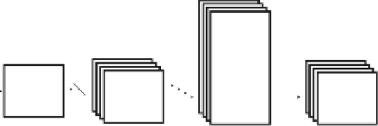
Four-Parallel MC Cache
Fig. 10.17
Proposed
four-parallel
MC cache
architecture
with four
independent
datapaths.
The hazard detection circuit is shown in detail
stage. Thus, while the reference data of a given block is being fetched, the previous
block is undergoing prediction. Note that the queue sizes here are decided based on
the behavior of the target DMA arbiter and DRAM latency, and for different systems
they should be optimized accordingly.
Since the cache system allows multiple pending reads, write-after-read hazards
are possible. For example, consider two MAUs A and B that are mapped to the same
cache line. Presently, the cache line contains A, the write queue contains a pending
cache miss for B and the read queue contains pending requests for A and B in that
order. If B arrives from the DRAM, it must wait until A has been read from the
cache to avoid evicting A before it has been read. The Hazard Detection Circuit in
Fig.
10.17
detects this situation and stalls the write of B.
10.6.2.3
Cache Parameters
Figures
10.15
b, c show the hit-rates observed as a function of the cache size and
associativity respectively. A cache size of 16 kB was chosen since it offered a good
compromise between size and cache hit-rate. The performance of FIFO replacement
is as good as Least Recently Used replacement due to the relatively regular pattern of
reference pixel data access. FIFO was chosen because of its simple implementation.
The cache associativity of 4 is sufficient to accommodate both Random Access GOP
structures and the three component planes (Y, U, V).