Hardware Reference
In-Depth Information
memory. The program counter (PC) is a counter that keeps the instruction address;
observe the write-PC (
wrPC
) control input. Finally, the instruction register is respon-
sible for storing and decoding the instructions; note the write-instruction-register
(
wrIR
) control input.
The control unit, shown in the lower part of the i gure, is responsible for producing
all control signals. Its main input (besides clock and reset) is an opcode, based on
which the whole sequence of events needed for the datapath to perform the desired
computations is provided. An important aspect to observe is that the control unit,
although responsible for sequencing all of the computations, does not access the
data directly (except for some occasional trivial data monitoring). Instead, it just
makes the proper path manipulations such that the datapath itself produces the
intended results.
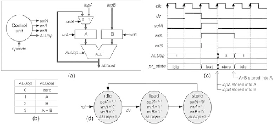
A simple datapath is depicted in i gure 3.22a, containing an ALU, two registers (A,
B), and a multiplexer. Four control signals are involved:
selA
(selects the data source
for register A),
wrA
and
wrB
(enable writing into registers A and B, respectively—at the
next positive clock edge), and
ALUop
(some of the ALU operations are listed in i gure
3.22b). These four control signals must be generated by the control unit, based on
opcode
. For simplicity, clock and reset are generally omitted in datapath representations
(as in i gure 3.22a), but they are obviously needed.
As an example, say that the following computation must be performed by the data-
path of i gure 3.22a: When an external input, called
dv
(data-valid bit), is asserted
Figure 3.22
(a) Datapath example. (b) Partial ALU's opcode table. (c) Illustrative timing diagram for the fol-
lowing computation: inputs are stored into A and B, then added, with the result then stored into
A. (d) Corresponding Moore machine.