Hardware Reference
In-Depth Information
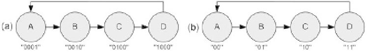
Figure 3.11
Four-state counter encoded with (a) one-hot and (b) sequential code.
i gure 3.11b, now using regular sequential encoding.
Because the number of states is a power of two, all possible two-bit values belong to
the machine; since all internal states are deadlock-free, the whole machine is deadlock-
free. It is important to mention, however, that with sequential or Gray encoding full
code usage is not needed for an outside initial state to eventually converge to one of
the actual machine states, thus without deadlock.
Deadlock prevention is necessary in any FSM, but in many applications it is also
required that the FSM start from a specii c state and with proper transition control
conditions. For example, one might want the FSM used to implement a trafi c light
controller to start from a state that keeps the lights red in all directions for a few
seconds (on power-up, after an energy failure, for example) before it proceeds to its
regular operation. This requires an explicit reset signal if the DFFs initial state is
arbitrary.
It is important to mention that there are devices (such as Altera's and Xilinx's
FPGAs) whose DFFs are automatically reset to '0' on power-up. In that case, if the all-
zero codeword belongs to the code and is assigned to the intended initial state, the
FSM will be reset automatically.
Still regarding the FPGAs mentioned above, whose DFFs' initial state is '0', note
that that does not reset the machine automatically when one-hot encoding is
used (see in i gure 3.11a that “0000” is not part of the codewords list). However,
contrary to Xilinx's XST synthesis compiler (of the ISE suite), which uses true
one-hot code, Altera's Quartus II synthesis compiler uses the modii ed one-hot
code seen in i gure 3.10b, which does include the all-zero codeword, thus allowing
automatic reset.
Figure 3.12 shows typical sources for the reset signal. In
Another example is shown in
i gure 3.12a it is generated
by a resistor-capacitor (RC) circuit; when the power is turned on, the voltage on C is
zero, so the full
V
DD
voltage is applied to the
rst
input, resetting the circuit; the voltage
on C then grows (with a time constant R
C = 0.1 s), thus eventually reducing the
voltage on R (
rst
) to zero and so freeing the circuit from the reset command. In i gure
3.12b, a specialized integrated circuit is used to generate the reset signal; if
V
DD
falls
below a predei ned threshold voltage,
rst
= '1' is produced, resetting the target circuit.
Finally, in i gure 3.12c, the reset signal is produced by another circuit that might
belong to the same system as the FSM (for example, another FSM to which this one
⋅