Hardware Reference
In-Depth Information
ignations for reset and clear are not universal; for instance, FPGA companies usually
call both “clear.” The diagram in i gure 2.2c shows how clear can be implemented;
note that when
clr
= '1',
d
is forced to '0', so at the next positive clock edge this '0'
will be copied to
q
, clearing the output.
Examples of functional response for both cases are included in i gure 2.2. Arrows
were placed on the clock waveforms to highlight the only moments at which the DFFs
are transparent. As can be seen, the value of
d
is copied to
q
at each of these clock
transitions. Note, however, that when
rst
is asserted (i gure 2.2a), the output is forced
to zero immediately, whereas when
clr
is asserted (i gure 2.2b), the output is forced to
zero at the next positive clock transition.
The
timing
response (with propagation delays taken into account) of a DFF is illus-
trated in i gure 2.3. A DFF with reset, similar to that of i gure 2.2a, was considered.
The propagation delays are dei ned in i gure 2.3a, where
t
pCQ(HL)
and
t
pCQ(LH)
represent
the propagation delays from
clk
to
q
(time interval between the clock edge and the
settling of
q
in the high-to-low and low-to-high transitions, respectively) and
t
pRQ
is
the propagation delay between
rst
and
q
. In the example of i gure 2.3b, the following
values were assumed:
t
pCQ(HL)
=
t
pCQ(LH)
= 2 ns and
t
pRQ
= 1 ns (note the gray shades in
the
q
waveform; the distance between the vertical lines is 1 ns).
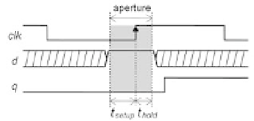
A i nal pair of time-related parameters dei ne the DFF's
forbidden
region (also called
aperture
or
transparency window
). As shown in i gure 2.4, such parameters are called
t
setup
and
t
hold
, which specify, respectively, how long before and after the clock edge the
Figure 2.3
(a) Time-related parameters of a DFF. (b) Example of
timing
response with
t
pCQ(HL)
=
t
pCQ(LH)
= 2 ns
and
t
pRQ
= 1 ns.
Figure 2.4
DFF's forbidden region (
d
must remain stable within the aperture window).