Hardware Reference
In-Depth Information
and '0', with the i rst bit considered to be the LSB, hence resulting
y
(3:0) = “0101”
after the pointer's 0-to-4 run is completed.
15.5 SPI Interface for an FRAM
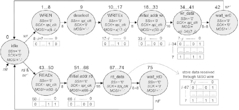
A i nal example is presented in i gure 15.6, which is an equivalent (pointer-based)
implementation for the FRAM SPI interface circuit studied in section 14.3.3. Note that
the machine of i gure 15.6 is exactly the same as that in i gure 14.20, just with the
adjustments needed for pointer-based implementation (main pointer
i
ranging from
0 to 75, secondary pointer
j
ranging from 0 to 7). The values (either 8 or 8
8) under
the arrows indicate the number of clock cycles spent in the preceding state (which is
the same as the number of bits transmitted or received in that state).
Observe that the enumeration of the states was done differently from that in
×
i gure
15.2 (just to illustrate another alternative). In state 1 of
i gure 15.2, for example, the
main pointer (
i
) stays i xed (
i
= 1), whereas the secondary pointer (
j
) sweeps the data.
Here, in state WREN, for example,
i
sweeps the data, while
j
is not used (so only in
states
wr_data
and
rd_data
are both pointers needed). Recall that, as in all FSM designs,
the crucial point is to develop a complete and precise state transition diagram (as
in i gure 15.6), after which any of the implementation techniques can be applied
straightforwardly.
Figure 15.6
FSM for the FRAM SPI interface circuit seen in section 14.3.3 (i gure 14.20), with all adjustments
for pointer-based implementation. Values under the arrows indicate the number of clock cycles
spent in the preceding state.