Hardware Reference
In-Depth Information
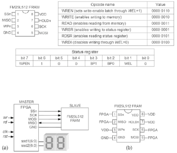
Figure 14.18
FM25L512 FRAM memory: Pinout, opcodes, and status register.
Figure 14.19
(a) Setup for the experiment. (b) FRAM wiring.
Note in i gure 14.18 that besides the SPI pins (
SCK
,
SSn
,
MOSI
,
MISO
), the chip
contains also two other control pins, called
WPn
(write protect) and
HOLDn
. The
purpose of
WPn
is, together with bits 7 (
WPEN
), 3 (
BP1
), and 2 (
BP0
) of the status
register, to allow several protection modes against writing to both the memory and
the status register. For example, with
WPn
= '1' and
WPEN
=
BP1
=
BP0
= '0', all writ-
ings are allowed (see other protection options in the device's datasheets). The role of
HOLDn
is to handle interrupts.
In addition to the bits mentioned above, there is another programmable bit in the
status register, called
WEL
(write enable latch), which determines whether writing is
allowed (when '1') or not (when '0'). Only when
WEL
= '1' are the protection options
mentioned above in place (any writing is forbidden while
WEL
= '0'). Because this bit
is automatically zeroed at power up or at the upward transition of
SSn
after a WRITE,
WRSR, or WRDI opcode, any write action must start with the WREN opcode because
that is the only way of setting
WEL
to '1' (writing to the status register does not affect
this bit).
Figure 14.19 shows the setup for the experiment. The inputs are
wr
(write) and
rd
(read) commands plus the traditional clock (assumed to be 50 MHz) and reset (
wr
,
rd
,