Hardware Reference
In-Depth Information
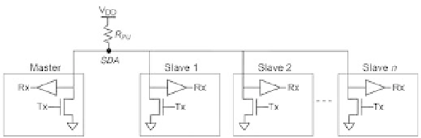
slave units. A common ground wire (not shown) is obviously also needed for the
system to function. Examples of IC families currently fabricated with I
2
C support are
also shown in the i gure, including microcontrollers, EEPROM and Flash memories,
A/D and D/A converters, RTC (real time clock) circuits, temperature sensors, and
accelerometers, among others.
As indicated in i gure 14.6, the clock (
SCL
) is unidirectional, always generated by
the master (usually a microcontroller), whereas data (
SDA
) transmission is bidirec-
tional. Because
SCL
and
SDA
are open-drain lines (the 5-Mbps version also allows
push-pull logic), external pull-up resistors (
R
PU
) must be connected between these wires
and the power supply.
The number of devices sharing the same bus can be up to 128 (seven-bit address)
or 1024 (10-bit address). More than one master is allowed, in which case the I
2
C pro-
tocol provides bus arbitration. Other advanced features include clock stretching,
general call, reset by software, and others.
14.2.2 Open-Drain Outputs
As mentioned,
SCL
and
SDA
are open-drain pins. Details on open-drain connections
for
SDA
(which is bidirectional) are shown in i gure 14.7. Note that for an individual
stage (the master, for example) to have its output high, the corresponding nMOS
transistor must be cut off (so its gate voltage must be low), because then the output
voltage will be elevated to
V
DD
by the pull-up resistor. Because all stages are hardwired
to the same
SDA
node, the only way to have
SDA
high is to have all nMOS transistors
off; in other words, all individual outputs must be high. Consequently, the
SDA
node
behaves as an AND gate, so any nonactive unit must keep its output high (i.e., internal
nMOS transistor gate voltage low) in order not to interfere with the communication
between any other units.
Because of the open-drain arrangement, the high-impedance state ('Z', in VHDL)
provided by tristate buffers is actually not needed. However, the design example
shown ahead is tested with the master on an FPGA (without open-drain pads), so in
that case the 'Z' state is required.
Figure 14.7
Open-drain connections for the
SDA
wire.