Hardware Reference
In-Depth Information
needed in the VHDL code to incorporate the following feature: the door must close
automatically 30 s after arriving at the completely open position. This feature should
be optional, so an input must be added to the circuit to allow the user to choose between
enabling it or not. How many DFFs will be needed to build the entire circuit now?
Exercise 9.8: Traffi c Light Controller
This exercise concerns the trafi c light controller of i gure 8.20c.
a) Which of the two timer control strategies (#1, section 8.5.2, or #2, section 8.5.3),
if any, can be adopted to implement this FSM?
b) Implement it using VHDL. Check whether the number of DFFs inferred by the
compiler matches the prediction made in section 8.11.5 for each encoding option
(sequential, Gray, Johnson, and one-hot). Recall that the predictions must be adjusted
in case the clock frequency is different from 50 MHz.
c) Physically test your design in the FPGA development board. Use three switches to
produce
stby
,
test
, and
rst
, and six LEDs to display the outputs.
d) At this point add the following feature (modify the design and download it to the
FPGA board): the yellow lights should blink (at 0.5 Hz) while the circuit is in the
standby mode.
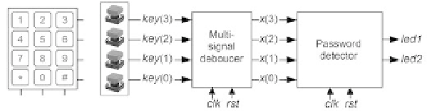
Exercise 9.9: Password Detector
This exercise concerns the password detector of i gure 8.22. A general block diagram
for the present design is shown in i gure 9.5, where, to ease the experiment, four
pushbuttons (from the FPGA board itself) replace the keypad. A multisignal debouncer
(treated in exercise 8.9) is also included. Only the following values are valid inputs (
x
)
to the password detector: “1111” (no pushbutton pressed), “0111” (top pushbutton
pressed), “1011”, “1101”, and “1110” (bottom pushbutton pressed).
a) Solve exercise 8.9 if not done yet.
b) Present a state transition diagram for each FSM to be used in this design.
c) How many DFFs are needed to build the entire circuit? Adopt a 1-ms debouncing
interval and sequential encoding for the FSMs. Check the clock frequency in your
FPGA development board.
Figure 9.5