Biomedical Engineering Reference
In-Depth Information
Next, a second pin-actuation sequence is applied to route droplets to their
target wells. The overall routing steps takes little time because all the wells
can be filled using only two pin-actuation sequences.
6.1.3 Chip Testing
To ensure reliability, the proposed chip design needs to be tested thoroughly.
We only focus here on a structural test where the goal is to route the test
droplet to traverse the target array for defect detection. In this section, we
discuss the adaptation of the parallel scan-like test presented in Chapter 4
(Subsection 4.1.1) to our chip design.
As presented in Chapter 4, the parallel scan-like test includes a cost-effec-
tive fault detection and a rapid diagnosis method based on test outcomes.
Given a microfluidic array, the scan-like test is carried out in parallel using
multiple droplets. Each column/row in the array is associated with a test
droplet and its “target region.” A target region for a droplet includes the cells
that are traversed by this droplet.
Here we adapt the parallel scan-like method to a well-plate design. As men-
tioned in Subsection 6.1.1, our well-plate design can be viewed as a special
case of a two-dimensional array where parts of the array are occupied by
wells and segregation walls. Unoccupied electrodes between wells are used
as transportation pathways.
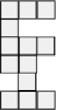
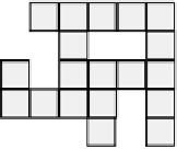
We focus on the testing of the transportation pathway since defects in the
transportation pathway will not only block well loading but also affect drop-
let routing among different well units. Note that the transportation pathways
are in fact composed of columns/rows of electrodes. Therefore, we should be
able to test these transportation pathways in parallel in the same way as the
columns and row test in the proposed parallel scan-like test procedure, as
shown in Figure 6.11.
Source
Capacitive sensing
circuit
Sink
Figure 6.11
Parallel scan-like test on multiwell chip.