Chemistry Reference
In-Depth Information
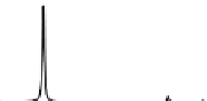
Fig. 12.9 Schematic
electronic structures and
charge-transfer excitations in
the CDW and CP phases
CDW
GS
X
P
MM
P
MXM
X
X
CP
GS
X
P
MXM
X
P
MM
X
a
c
U
M
=2,
V
MM
=1,
V
MXM
=0.5
b
U
M
=4,
V
MM
=2,
V
MXM
=1
U
M
=6,
V
MM
=3,
V
MXM
=1.5
AV
AV
AV
CDW
CDW
CDW
CP
CP
CP
0
1
2
3
4
0
1
2
3
4
0
1
2
3
4
ω
ω
ω
Fig. 12.10 Optical conductivity in the AV, CDW, and CP phases of the 12-site model for
(a)
U
M
¼
2,
V
MM
¼
1, and
V
MXM
¼
0.5, (b)
U
M
¼
4,
V
MM
¼
2, and
V
MXM
¼
1, and
(c)
U
M
¼
6,
V
MM
¼
3, and
V
MXM
¼
1.5. The other parameters are
t
MM
¼
1,
t
MXM
¼
0.8,
a ¼
0.2,
b ¼
4,
y
0
¼
0.1, and
V
2
¼
0[
23
]
Among the energies of the experimentally observed peaks, that in the CDW
phase is lower than those in the CP phase. The energy difference between the
CDW and CP phases is reproduced in Fig.
12.10
for each parameter set. This
is easily understood in the strong-coupling limit. The low-energy charge-transfer
excitation takes place at
E
CDW
MXM
¼
bjyjV
MM
þ
2
V
2
in the CDW phase and at
2
E
C
MM
¼
2
V
2
in the CP phase. We concluded above that the nearest-
neighbor repulsion through an X site
V
MXM
is substantially weaker, at least for the
2
bjyjþV
MXM


Search WWH ::

Custom Search