Hardware Reference
In-Depth Information
Discovering the I2C protocol
Every chip on the CryptoCape uses the
Inter-Integrated Circuit
(
I2C
) Bus. I2C was deve-
loped by Phillips Semiconductor over 20 years ago, but it is still very prevalent in electron-
ics design today. I2C requires two signal lines, one for a
Serial Clock
(
SCL
) and the other
for
Serial Data
(
SDA
). Devices attached to the bus are either classified as master or slave.
Each slave device has an address and there can be more than one master. The I2C protocol
supports collision detection and is a true multimaster protocol.
The SDA and SCL lines are
pulled up
to the system voltage, VCC, typically with resistors
connected from VCC to SDA and VCC to SCL. The processor on the BBB, the AM335x,
contains internal pull-up resistors for the bus. Data is encoded to the bus by manipulating
the logic levels of the SDA and SCL lines. For example, to start sending data, the master
pulls SDA low while holding SCL at a logic high. The stop condition is sent with a low to
high transition of SDA while holding SCL high.
Note
Revision 6 of the I2C bus specification can be found on NXP semiconductors (previously
Phillips) website at
http://www.nxp.com/documents/user_manual/UM10204.pdf
.
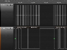
The following screenshot shows a normal I2C operation as captured by a logic analyzer. A
logic analyzer
is an instrument that can sample electrical connections and often decode the
signals to produce a human readable format.