Hardware Reference
In-Depth Information
Pin
Name
Description
Pin
Name
Description
A86
AD38
Address/Data 38
B86
AD39
Address/Data 39
A87
GND
Ground
B87
AD37
Address/Data 37
A88
AD36
Address/Data 36
B88
+
5 V
Power (
+
5V or
+
3.3 V)
A89
AD34
Address/Data 34
B89
AD35
Address/Data 35
A90
GND
Ground
B90
AD33
Address/Data 33
A91
AD32
Address/Data 32
B91
GND
Ground
A92
RES
Reserved
B92
RES
Reserved
A93
GND
Ground
B93
RES
Reserved
A94
RES
Reserved
B94
GND
Ground
Notes:
1
Signals on pins 63 to 94 are only used on 64-bit PCI bus cards.
2
The copper foil side of the card is side A whilst the component side is side B.
3
A # used after a signal name indicates that the signal in question is active
low (or asserted low).
4
The time-multiplexed address and data bus may exist as either 0 to 31 bits
(32 bits) or 0 to 63 bits (64 bits) using the 64-bit expansion bus. Both address
and data signals use the same bus; addresses followed by data. A 32-bit PCI
may also use 64-bit addressing by using two address cycles, referred to as
Dual Address Cycles (DAC), in which the low order address is sent first.
Additional control bits are used when the bus is used in 64-bit mode.
5
The bus connectors are labelled '
+
5V
or
+
3.3 V' in the case of
+
5 V systems
and '
+
3.3 V' for 3.3 V systems. Note that the original PCI standard required
that plug-in boards use
+
5 V supplies provided by the PCs motherboard. As
the PCI standard evolved, the option was added for a
+
3.3 V power source.
Furthermore, the newer PCI 2.3 standard has now made the
+
5 V supply
obsolete. This means that many of the most recent PCs can only accept 3.3 V
or 'universal' PCI cards. Contacts on the PCI connector (keyways A12, B12,
etc.) are used to determine the correct power rail voltages (see Figure 2.2).
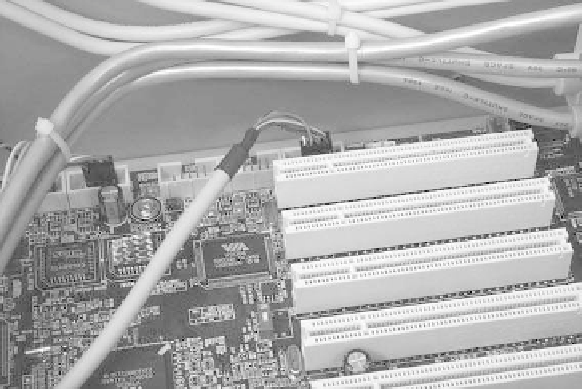
Photo 2.13
Five PCI expansion connectors in a modern PC