Hardware Reference
In-Depth Information
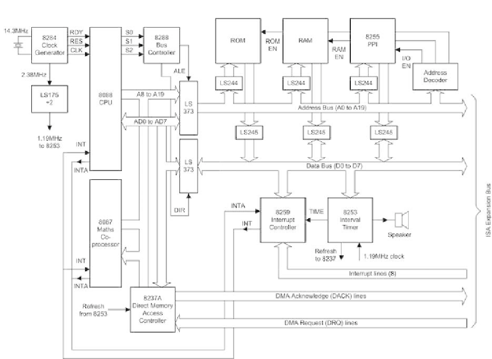
Figure 1.10
Internal architecture of the original IBM PC
The system address bus (available on each of the expansion connectors)
comprises 20 address lines, A0 to A19. The system data bus comprises eight
lines, D0 to D7. Address and data information are alternately latched onto the
appropriate set of bus lines by means of the four 74LS373 8-bit data latches.
The control signals, ALE (address latch enable), and DIR (direction) derived
from the 8288 bus controller are used to activate the two pairs of data latches.
The CPU bus is extended to the 8087 numeric data processor (maths copro-
cessor). This device is physically located in close proximity to the CPU in order
to simplify the PCB layout.
The original PC required a CPU clock signal of 4.773 MHz from a dedi-
cated Intel clock generator chip. The basic timing element for this device is a
quartz crystal which oscillates at a fundamental frequency of 14.318 MHz. This
frequency is internally divided by three in order to produce the CPU clock.
The CPU clock frequency is also further divided by two internally and again
by two externally in order to produce a clock signal for the 8253 Programmable
Interrupt Timer. This device provides three important timing signals used by the
system. One (known appropriately as TIME) controls the 8259 Programmable
Interrupt Controller, another (known as REFRESH) provides a timing input for
the 8237 DMA Controller, whilst the third is used (in conjunction with some
extra logic) to produce an audible signal at the loudspeaker.