Hardware Reference
In-Depth Information
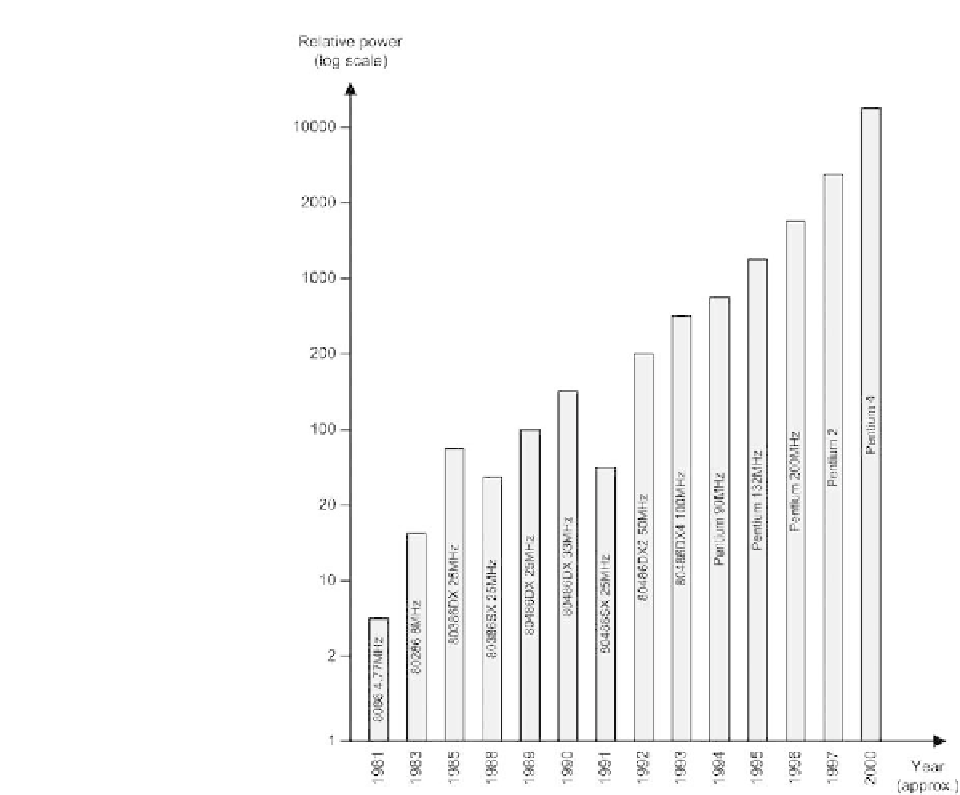
Figure 1.9
Relative power of Intel processors over the last two decades
integrated chipsets are usually a superset of those provided by the much larger
number of devices found in their predecessors.
There is more to Figure 1.10 than mere historical interest might indicate as
modern PCs can still trace their origins to this particular arrangement. It is,
therefore, worth spending a few moments developing an understanding of the
configuration before moving on to modern systems that employ a much faster
multiple bus structure.
The 'CPU bus' (comprising lines A8 to A19 and AD0 to AD7 on the left
side of Figure 1.10) is separated from the 'system bus' which links the support
devices and expansion cards.
The eight least significant address and all eight of the data bus lines share
a common set of eight CPU pins. These lines are labelled AD0 to AD7. The
term used to describe this form of bus (where data and address information take
turns to be present on a shared set of bus lines) is known as 'multiplexing'. This
saves pins on the CPU package and it allowed Intel to make use of standard
40-pin packages for the 8088 and 8086 processors.