Hardware Reference
In-Depth Information
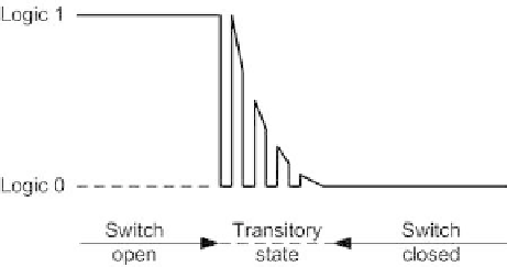
Figure 9.3
Typical waveform produced by a switch closure
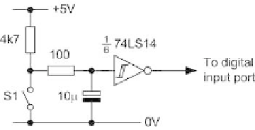
Figure 9.4
Simple debounce circuit
shows the waveform generated by the simple switch input circuit of Figure 9.1
as the contacts close. The spurious states can cause problems if the switch is
sensed during the period in which the switch contacts are in motion, and hence
steps must be taken to minimize the effects of bounce. This may be achieved by
means of additional hardware in the form of a 'debounce' circuit or by including
appropriate software delays (of typically 4 to 20 ms) so that spurious switching
states are ignored. We shall discuss these two techniques separately.
Hardware debouncing
Immunity to transient switching states is generally enhanced by the use of active-
low inputs (i.e. a logic 0 state at the input is used to assert the condition required).
The debounce circuit shown in Figure 9.4 is adequate for most toggle, slide, and
push-button type switches. The value chosen for R2 must take into account the
low-state sink current required by IC1 (normally 1.6 mA for standard TTL and
400
µ
A for LS-TTL). R2 should not be allowed to exceed approximately 470
in order to maintain a valid logic 0 input state. The values quoted generate an
approximate 1 ms delay (during which the switch contacts will have settled into
their final state). It should be noted that, on power-up, this circuit generates a
logic 1 level for approximately 1 ms before the output reverts to a logic 0 in the
inactive state. The circuit obeys the following state table:
Switch condition
Logic output
closed
1
open
0