Environmental Engineering Reference
In-Depth Information
The voltage gain is inverting, and neglecting the input loss, is reduced to
when the device output resistance, is much higher than the load
resistance, Conversely, it achieves its maximum value, which
depends only on bias conditions and technological parameters, when the load
resistance is much higher than the transistor output resistance. Also for this
reason, quantity
is said to be the
intrinsic voltage gain
of the
configuration.
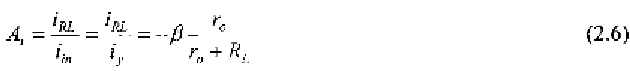
The current gain is defined as the ratio between the current flowing into
the Y terminal and that flowing in the load resistor to ground. It has a finite
value only for bipolar devices and is strictly related to parameter in (2.4).
Its magnitude decreases to a value lower than when the output resistance
cannot be considered much higher than the load resistance
2.4 COMMON X WITH DEGENERATIVE RESISTANCE
The common X configuration with a local resistive feedback
is shown
in Fig. 2.5a.
Although the main concern of this topic is feedback, for the moment we
will not consider the effects of resistance from a feedback point of view,
but analyse it directly from the small-signal circuit illustrated in Fig. 2.5b.
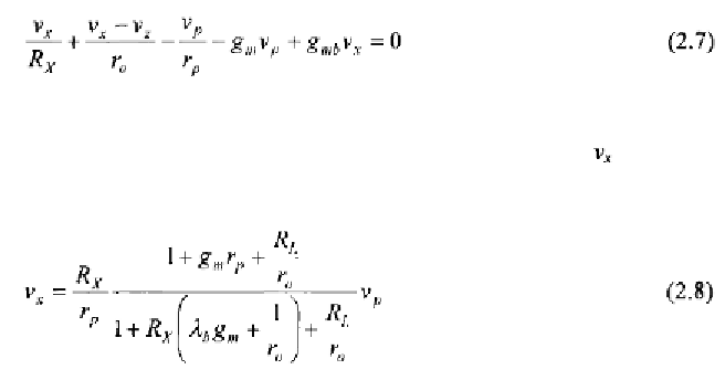
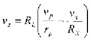
To find the input resistance of the CX configuration we apply the KCL at
terminal X
By considering that
and solving (2.7) for
we get