Environmental Engineering Reference
In-Depth Information
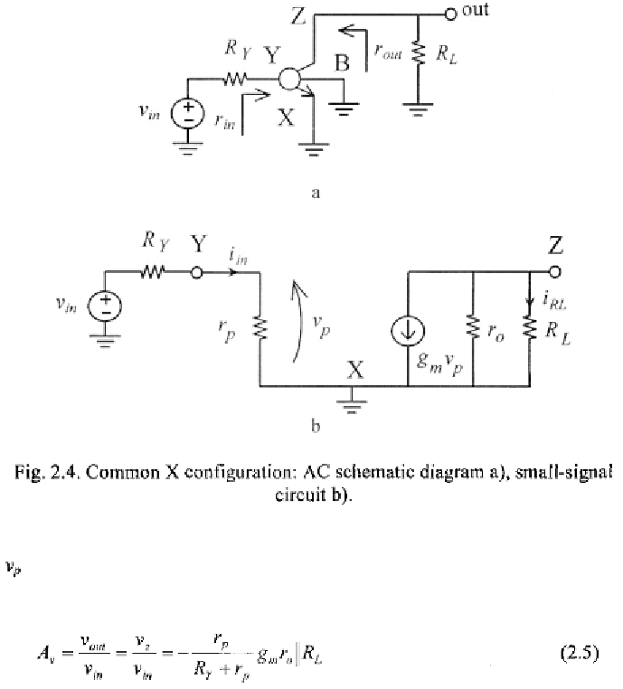
2.3 COMMON X (EMITTER/SOURCE) CONFIGURATION
Fig. 2.4a depicts the AC schematic diagram of the
common X
(CX)
configuration. This circuit is used to provide voltage and current gain. The
figure also includes resistance which would not be strictly necessary, to
render the analysis a more general one. It can account for the distributed
base resistance of bipolar devices or the internal resistance of the signal
generator. The small-signal circuit is illustrated in Fig. 2.4b. By defining the
input and the output resistances of the common X configuration as illustrated
in Fig. 2.4a, we can simply see by inspection that these are
and
respectively.
Voltage gain between terminal Y and Z can be evaluated considering that
equals
and taking into account the input coupling between
and
leading to the overall voltage gain