Environmental Engineering Reference
In-Depth Information
Chapter 2
SINGLE TRANSISTOR CONFIGURATIONS
2.1
THE GENERIC ACTIVE COMPONENT
In order to ensure that all analytical results derived herein are applicable
to feedback configurations realised with both BJT and MOSFET
technologies -including heterostructure bipolar transistor (HBT) and III-V
compound metal-semiconductor field effect transistor (MESFET)
technologies- we introduce the generic transistor component, whose circuit
symbol and low-frequency small-signal model are shown in Fig. 2.1a-b and
Fig. 2.1c, respectively [PC981].
This device is identified by four terminals denoted as X, Y, Z and B.
Specifically, X, Y, and Z respectively representing the emitter, base, and
collector terminals for BJTs (and HBTs) or the source, gate, and drain of
MOSFETs (and MESFETs). The fourth terminal B represents the substrate
or bulk node, it is almost always biased at a fixed potential and conducts a
negligible static current. Symbols X, Y and Z were chosen to remind us of
the functional equivalence between our generic device and the
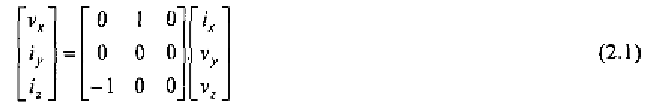
negative
second generation Current Conveyor
(CCII-) [SS70], [TLH90], [PPP99].
The ideal negative
1
CCII is a three-terminal device labelled by X, Y and Z
(see Fig. 2.2) and is characterized by the following port relation
1
In a positive CCII the direction of the current flow at terminal Z has an opposite
sign to a CCII-, i.e.