Environmental Engineering Reference
In-Depth Information
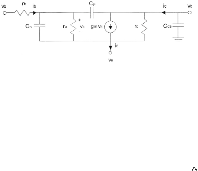
All the above dc small-signal components are intrinsic terms of any BJT
since they depend on the npn junction itself.
The model in Fig. 1.18 also includes a base resistance, which comes
out in a real implementation. Specifically, models the resistive path that
exists between the effective transistor base region (i.e. the gray area in Fig.
1.16) and the base contact (i.e. the p+ doped region). This path presents a
small ohmic resistance of a few tens or hundreds of ohm. With respect to
has a small value and, in low frequency operations, it can be neglected
since the base-emitter voltage is practically equal to In high-frequency
circuits (i.e. in RF applications), part of the base current flows across
thus
reducing the effective impedance in the base-emitter branch. Because of the
presence of
can be significantly different from the base-emitter voltage
applied thus considerably affecting transistor properties. In practice,
cannot be neglected if a high-speed circuit is being analyzed or designed.
Note that there is also an ohmic resistance in series with the actual
collector (whose value is lowered by the n+ buried layer) but its presence is
not as crucial as the base resistance is.
As far as the capacitive contribution is concerned, we have two main
intrinsic capacitors,
and
as well as capacitor,
which exists in
integrated implementations only.
Specifically, capacitor is the base-emitter capacitor and is expressed
by (1.86), while which represents the base-collector capacitive
contribution, is expressed by (1.87). Due to their nature, is at least one
order of magnitude smaller than and, in several cases, is neglected.
However, its contribution becomes significant when a high gain exists
between the base and the collector.
Capacitor comes out from the reverse biased pn region realized by
the collector-substrate junction. This capacitor is quite large and is modeled
by the following expression