Environmental Engineering Reference
In-Depth Information
Since the capacitor is mainly determined by the gate-channel
capacitance and the overlap effect can be neglected in many cases.
The same boundary effect that determines the gate-source
overlap
capacitance yields the gate-drain capacitance that is given by
This capacitor makes a strong contribution when the transistor is used as a
voltage amplifier and a large voltage gain exists between the drain and the
gate. In all other cases its contribution is negligible.
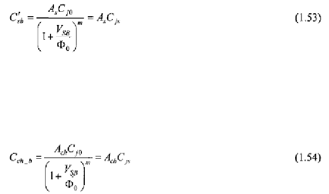
The second largest capacitor is the source-bulk capacitor, which can be
split into three contributions all of them given by the depletion capacitances
of reverse biased pn junctions. The
takes into account the junction
capacitance between the n+ source area and the bulk. Its expression is
similar to (1.13) or (1.16) depending on whether the junction can be
considered as abrupt or graded. Assuming a graded junction we have
first,
where
is the area of the source junction and
is defined as the source
junction capacitance per unit area.
The second contribution is responsible for and takes into account the
depletion region between the channel and the bulk. Even in this case we
have an expression similar to (1.53) that is
where is the area of the channel which can be evaluated as
WL.
The third term is referred to as the source-bulk sidewall capacitance and is
denoted as This capacitance is due to the presence of a highly p+
doped region (field implant) that exists under the thick field oxide (FOX)
and prevents the leakage
current from flowing between two adjacent
transistors. The value of
can be particularly large if the field implant is
heavily doped as in modern technologies. The expression of
is then