Environmental Engineering Reference
In-Depth Information
critical source. Since is made infinitely large, current
i
tends to zero.
Thus the same current flows into and and since voltage appears at
the inverting terminal (thanks to the input voltage follower) a virtual short-
circuit appears between the inverting and the non inverting terminals. The
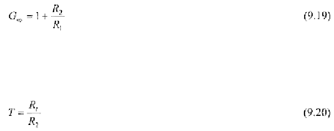
asymptotic closed loop gain is hence
which is the same result we would have obtained using a VOA in place of
the CFOA.
In addition, the loop gain is
showing that the loop gain depends on the transresistance gain, and on
only one of the two external resistances, Since the closed-loop bandwidth
is proportional to the loop gain, and the closed-loop gain can be set by
changing only
a closed-loop constant bandwidth behavior is achieved.
9.5
TRANSISTOR-LEVEL ARCHITECTURE, SMALL-SIGNAL
MODEL, AND FREQUENCY COMPENSATION OF CFOAs
According to the architecture in Fig. 9.9, a CFOA is made up of three
main blocks: two voltage buffers and one current buffer. More specifically,
the first voltage buffer is located at the input and its output current is
replicated by the current buffer into a high-impedance internal node. The
other voltage buffer is at the output with the purpose of properly driving the
output load.
The simplified circuit schematic of a typical CFOA is represented in Fig.
9.13, where bipolar transistors are used [HR80], [TLH90]. The Load and
compensation capacitors, and and the feedback network made up of
resistors and are also included. The input voltage buffer is
implemented with transistors T1-T4 and associated bias current generators
Two current mirrors T5-T6 and T7-T8 implement the current buffer,
while transistors T9-T11 and generators
form the output voltage buffer.
Capacitor provides dominant-pole compensation. Nearly all monolithic
complementary
bipolar
high-speed
CFOAs are a variation of this
architecture [B97].