Environmental Engineering Reference
In-Depth Information
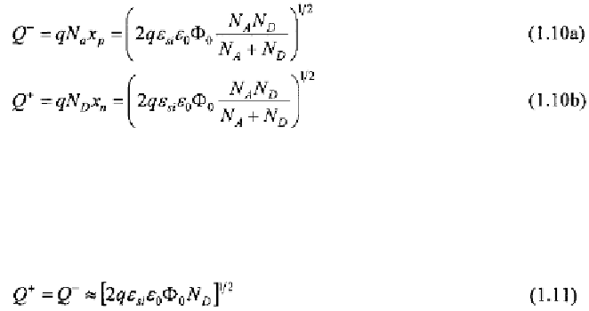
Note that the charge stored on the n side equals the charge stored on the p
side, as is expected due to the charge neutrality.
In the case of a more heavily doped side, as in our example where
we can simplify (1.10) to
1.2.1
Reverse Bias Condition
By grounding the anode and applying a voltage to the cathode, we
reverse-bias the device. Under such a condition the current flowing through
the diode is mainly determined by the junction area and is independent of
In many cases this current is considered negligible and the device is modeled
as an open circuit. However, the device also has a charge stored in the
junction that changes with the voltage applied and causes a capacitive effect,
which cannot be ignored at high frequencies. The capacitive effect is due to
the so-called junction capacitance.
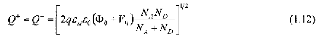
Specifically, when the diode is reverse biased as in Fig. 1.2, free electrons
on the n side are attracted by the positive potential and leave behind
positive immobile charges. Similarly, free holes in the p region move
towards the anode leaving behind negative immobile charges. This means
that the depletion region increases and that the built-in potential increases
exactly by the amount of applied voltage,
Given that the built-in potential is increased by both the width and the
charge of the depletion region can be found by substituting the term
to
in (1.7) and (1.10), respectively. In particular the charge stored results
as