Environmental Engineering Reference
In-Depth Information
in which can be evaluated by suitably modelling transistor T2
according to the method described in section 2.7.2 and using equation (2.46),
which yield
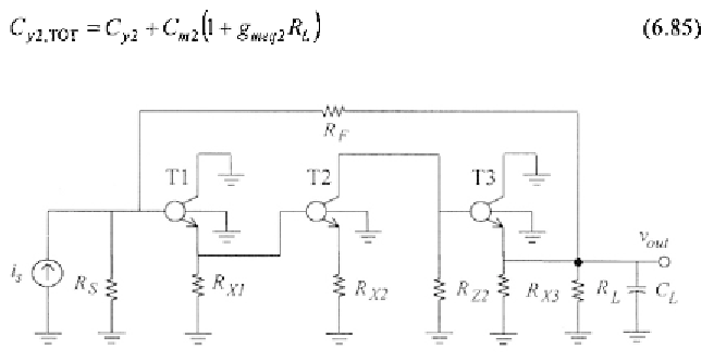
6.6.3 Frequency Compensation of the Shunt- Shunt Amplifier
To analyse the compensation of the shunt-shunt amplifier, for simplicity,
we will refer to the circuit in Fig. 6.35 instead of using the one in Fig. 6.19.
It exhibits only one amplifying stage (transistor T2) within two voltage
buffering stages provided by transistor T1 and T3. Thus, the equivalent
resistance at the gain stage input is low (that of terminal X1) and Miller
compensation becomes impractical. Instead, we have to use, dominant-pole
compensation at node Y3 which is the only high-impedance node. The
equivalent resistance which, associated with the compensation capacitor, sets
the dominant pole is
The second pole arises at the output terminal, as is associated with the
usually large load capacitance.
It is worth noting that the original scheme in Fig. 6.19 was made up of three
(inverting) gain stages. This structure usually includes three low-frequency
poles (two at the high-resistance internal nodes, Y2 and Y3, and one at the
output due to the high load capacitance). In this case, the most suitable