Environmental Engineering Reference
In-Depth Information
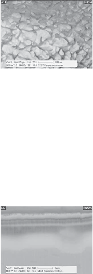
Figure 2.4
Surface with HTS sealing. Dense layer of acicular “petal”-shaped crystals. h e
pores are closed on the surface.
Figure 2.5
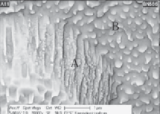
Surface etched with Ga ions. With the sealing removed, well distributed
pores with high tortuosity became visible. Pore diameter ~170 nm (outer) and 15-44 nm
(inner).
Figure 2.6
TSA with HTS. SEM imaging of the FIB cross-section coni rmed the
homogenous morphology (no pores) of the anodic layers. h e white stripes within them
are caused by the charging during SEM investigation. h e intensity modulation of these
stripes could be the result of dif erent conductivity (composition) of the layers.
Search WWH ::

Custom Search