Environmental Engineering Reference
In-Depth Information
UV Photon
Ag
Ag
Conducting Channel
Glass
(
a
)
Adsorbed
Oxygen layer
Wire boundary
UV light
(001)
(100)
(010)
(110)
(001)
GLASS
(
b
)
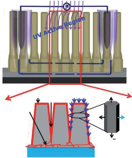
Figure 16.5
Cross-sectional schematic view of nanowire array photodetector: (a) the
charge transport takes place via bottom dense part of the NWS (called the conducting
channel); (b) Nanowire surfaces that have “O” species called as absorbed oxygen layer [25].
deposited using thermal coating unit which render metal semiconductor
metal (M-S-M) junctions with the nanowire i lms. Two terminals are used
to measure the current while the other two are used to apply voltage
h e electron transport mechanism is quite dif erent in nanowire array
i lms than in planer ZnO i lms. A schematic cross-sectional cartoon
(Figure 16.5) of a typical device depicts that nanowires are connected
through Ag metal on the top and the bottom layer of NWs, acting as the
conducting channel [25]. Transport properties of ZnO nanowire i lms
depend upon the interaction among the nanowires and their orientation.
h e increased density of oriented (002) crystallites (nanowire) in ZnO
i lm is associated with a reduction of large-angle grain boundaries; and
it reduces scattering of charge carriers and increases the mobility of ZnO
NWs i lm [161, 162]. h e large-size grains (NW diameter) which attach
Search WWH ::

Custom Search