Environmental Engineering Reference
In-Depth Information
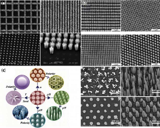
Figure 16.2
(a) E-beam lightraphically patterned ZnO nanorod [76]. (b) Nanoscale
two-dimensional patterns of ZnO nanorods using laser interference lithography [74].
(c) polymer-templated hydrothermal growth of patterned ZnO nanorods and various
morphologies [80]. (d) Sot chemical templated (polystyrene sphere and TiO2 layer)
control growth of ZnO nanowires [75].
needle-like, tubular, tree-like, and spherical shapes are obtained by con-
trolling the growth conditions. Figure 16.2c represents various morpholo-
gies of ZnO nanostructures which utilized various growth conditions and
structural polarity [74]. A direct patterning of ZnO nanoparticle (NP)
seeds via microcontact printing demonstrated excellent spatial control
over nanowire growth in a large area, which can also be performed on
l exible substrates to be utilized in l exible electronic devices [79]. h is
kind of printing needs master stamps with dei ned structures, the con-
centration and viscosity of ink (seed solution) plays an important role
on pattern quality [81]. h ough top-down approaches to patterning have
shown superb control over patterns, these processes are very time con-
suming and require high cost tools and excellent operating skills. Hence,
the sot chemical-based self-assembled monolayer approach is becoming
quite attractive for large-scale and low-cost patterning. Monolayer of PS
Search WWH ::

Custom Search