Environmental Engineering Reference
In-Depth Information
(a)
(b)
-1.0
-0.5
0
0.5
1.0
1.5
2.0
2.5
3.0
3.5
-1.0
-0.5
0
0.5
1.0
1.5
2.0
2.5
3.0
3.5
e
-
e
-
e
-
e
-
e
-
e
-
(2)
CB
CB
e
-
e
-
e
-
e
-
e
-
e
-
CB
CB
(1)
(1)
(3)
(2)
(3)
h
+
h
+
h
+
h
+
h
+
h
+
VB
VB
(4)
n-Cu
2
O
p-Cu
2
O
h
+
h
+
h
+
h
+
h
+
h
+
VB
VB
WO
3
WO
3
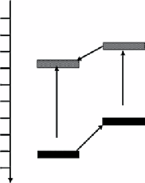
figure 3.12
Schematic diagram for the charge-transfer process in WO
3
/n-Cu
2
O composite film (a) and in WO
3
/p-Cu
2
O composite
film (b). Reproduced by permission from Ref. [147]. © 2012, elsevier B.V.
well in the decomposition of organic contaminants. The efficiency for this kind of photocatalytic system is related to the ratio
of TiO
2
and Cu
2
O in the composite. When the amount of TiO
2
in the composite is very close to that of Cu
2
O, almost all of the
electrons generated from Cu
2
O have place to transfer. If the amount of TiO
2
is much higher than that of Cu
2
O, a significant
number of the electrons generated from Cu
2
O under VL cannot be transferred, leading to low efficiency for dye degradation, or
the inability to produce enough H
2
O
2
.
Wei et al. [147] fabricated WO
3
/n-Cu
2
O and WO
3
/p-Cu
2
O composite films on titanium (Ti) substrates with a consecutive
cathodic electrodeposition route. They found that the photocatalytic activity of WO
3
/n-Cu
2
O was higher than that of WO
3
but
lower than that of n-Cu
2
O. On the contrary, WO
3
/p-Cu
2
O exhibited higher photocatalytic activity than both WO
3
and p-Cu
2
O
alone. The suppression of photocatalytic activity for n-Cu
2
O when it is combined with WO
3
can be interpreted using a sche-
matic diagram of energy band structure of the WO
3
/n-Cu
2
O film shown in Figure 3.12a. Under simulated natural light illumi-
nation, the electrons in the VB of Cu
2
O and WO
3
are excited to their corresponding CB according to processes (1) and (3) shown
in Figure 3.12a, respectively. The CB edge of Cu
2
O (−0.28V versus NHe) is higher than that of WO
3
(+0.4V versus NHe); the
VB edges of Cu
2
O and WO
3
are situated at +1.92 and +3.1V versus NHe, respectively [160, 161]. From the thermodynamic
viewpoint, the photogenerated electrons can transfer from CB of Cu
2
O to that of WO
3
(process (2)), while the photogenerated
holes can migrate in the opposite direction from VB of WO
3
to that of Cu
2
O (process (4)). Because it is impossible for the pho-
togenerated electrons in the CB of WO
3
to be consumed by the adsorbed oxygen through one-electron reduction, such a charge
transfer weakens the stronger reduction power of photogenerated electrons in the CB of Cu
2
O. As a result, the WO
3
/n-Cu
2
O
composite film shows photocatalytic activity lower than that of a single n-Cu
2
O film. This mechanism can also be used to
explain similar results obtained by others for ZnO/Cu
2
O and TiO
2
/Cu
2
O composite photocatalysts [162, 163]. For the WO
3
/p-Cu
2
O
composite film, it is more likely that the WO
3
/p-Cu
2
O composite film shows a different mechanism for photogenerated charge
transfer. This can be explained based on the model of the p-n photochemical diode shown in Figure 3.12b rather than the
charge separation model (shown in Fig. 3.12a). In this p-n heterojunction, the majority of electrons in WO
3
and the majority of
holes in p-Cu
2
O combine by transfer through the interface between the two semiconductors (process (3)), while the recombina-
tion of photogenerated charges in the respective semiconductors is suppressed. Consequently, the photogenerated electrons
with strong reduction power in the CB of Cu
2
O and the photogenerated holes with strong oxidation power in the VB of WO
3
are retained. In such a case, two photons must be absorbed to generate one net electron-hole pair for redox reactions at the
photocatalyst surface.
3.3.1.3.2 Noble Metal/Cu
2
O for Organics Degradation
Semiconductor/noble metal nanocomposites as photocatalysts have
been extensively studied [164-167]. It is believed that in these semiconductors/noble metals, photoexcited electrons in the CB can
be transferred to noble metals, which act as electron sinks due to the Schottky barrier at the metal/semiconductor interface, while
the holes can remain on the semiconductor surface [168]. The recombination of electrons and holes can therefore be prolonged and
the photocatalytic efficiency thereby improved [169]. In addition, the surface plasmon resonance of noble metal NPs is expected
to enhance the absorption of incident photons, which enhance the photocatalytic efficiency of semiconductors [170].