Environmental Engineering Reference
In-Depth Information
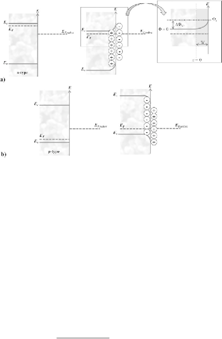
Figure 10.4.2
Schematic representation of the band bending effect for (a) an n-type semiconductor
and (b) a p-type semiconductor.
of transferred charge to the surface of the semiconductor and the density of shallow
donors in the semiconductor material,
N
D
.
d
2
d
x
2
1
εε
0
ρ
(
x
)
d
ξ
d
x
=−
=−
(10.4.11)
ε
and
ε
0
are the dielectric constant and the permittivity of free space, respectively.
ξ
is
the electric field and the total charge density
ρ
is given by (Krol and Grätzel, 2012):
e
[
N
D
−
ρ
(
x
)
=
n
(
x
)]
(10.4.12)
where
x
is the distance from the surface,
N
D
is ionized donor density, given by the
doping of the semiconducting material - Equation 10.4.9. The concentration of free
electrons,
n
(
x
) varies with distance - Equation 10.4.5.
Since the Fermi level is expected to be constant within the space charge region,
the position of the conduction band energy
E
C
(
x
) varies with the distance by the band
bending effect,
(
x
), as follows:
N
C
exp
n
0
exp
e
(
x
)
kT
−
−
E
C
(
x
)
E
F
e
(
x
)
n
(
x
)
=
−
=
(10.4.13)
kT

Search WWH ::

Custom Search