Image Processing Reference
In-Depth Information
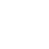
Quantum-dot
Tunnel Junction
Electron
"1"
"0"
Fig. 4.3
The two possible charge configurations of a QCA cell
external electrostatic influence, Coulomb repulsion will force the electrons to dots
on opposite corners [28, 29, 44, 62]. The two possible charge configurations are
presented in Fig. 4.3 and correspond to binary “1” and “0”.
In the following paragraphs, the implementations of the basic components of
QCA circuits will be presented. The binary wire, the inverter and the three-input
majority gate are fundamental components. The logic AND and OR gate are imple-
mented using the majority gate.
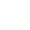
The successive placement of QCA cells one after the other in one direction, acts
like a wire and is usually called binary wire [28]. Fig. 4.4 presents the binary wire
component, where the input
A
that is fed in the left, is transmitted towards the right
direction to the output. In this example the input
A
equals to logic “0” as the elec-
trons are placed in the upper left and down right dots. In the second cell the elec-
trons, due to Coulomb repulsion, will have the same state as in the first cell. The
same happens in all the cells that follow in the same direction, so the last cell (the
output) will be in the same state “0” as the input. In the case that the input
A
changes
to logic “1”, the second cell will also change to “1”, due to Coulomb repulsion. The
same will happen successively to all cells and the output cell will also become “1” .
So, in any case, the input is transmitted to the output and this function simulates the
classical wire.
The three-input QCA majority gate is one of the most important processing ele-
ments in QCA circuits and its implementation was proposed in [62]. The majority
gate is constructed with a cross structure. The logic function of the three-input ma-
jority gate is
M
(
A
,
B
,
C
)=
AB
+
AC
+
BC
and the output has to be the same as the
,
,
majority of the three inputs
A
B
C
. The implementation is composed of five cells as
=
=
=
shown in Fig. 4.5. Here
A
0. The electrostatic forces between the
electrons of the three input cells constrain the electrons of the centric cell to get the
state of logic “0”. Generally, the state of the centric cell is set by electrostatic forces
from the logic state of the majority of the inputs. This state is then transmitted to the
output cell at the right.
1,
B
0and
C
A
A
Fig. 4.4
The QCA binary wire


Search WWH ::

Custom Search