Hardware Reference
In-Depth Information
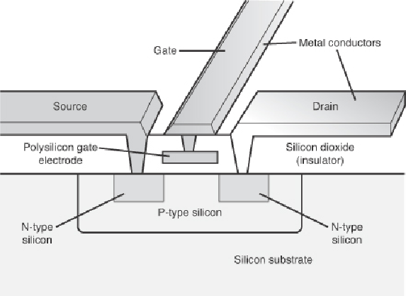
A PMOS transistor works in a similar but opposite fashion. P-type silicon is used for the
source and drain, with N-type silicon positioned between them. When a negative voltage
is placed on the gate, the gate electrode creates a field that repels electrons from the N-
type silicon between the source and drain. That in turn changes that area to behave as if it
were P-type silicon, creating a path for current to flow and turning the transistor “on.”
When both NMOS and PMOS field-effect transistors are combined in a complementary
arrangement, power is used only when the transistors are switching, making dense, low-
power circuit designs possible. Because of this, virtually all modern processors are de-
signed using CMOS (Complementary Metal Oxide Semiconductor) technology.
Comparedtoatube,atransistorismuchmoreefficientasaswitchandcanbeminiaturized
to microscopic scale. Since the transistor was invented, engineers have strived to make it
smaller and smaller. In 2003, NEC researchers unveiled a silicon transistor only 5 nano-
meters(billionthsofameter)insize.Othertechnology,suchasGrapheneandcarbonnan-
otubes, are being explored to produce even smaller transistors, down to the molecular or
even atomic scale. In 2008, British researchers unveiled a Graphene-based transistor only
1 atom thick and 10 atoms (1nm) across, and in 2010, IBM researchers created Graphene
transistorsswitchingatarateof100gigahertz,thuspavingthewayforfuturechipsdenser
and faster than possible with silicon-based designs.