Hardware Reference
In-Depth Information
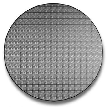
Figure 3.5
200mm (8-inch) wafer containing 177 full Pentium 4 Northwood (0.13-micron) processor
cores.
Chipsaremanufacturedfromthewafersusingaprocesscalled
photolithography
.Through
this photographic process, transistors and circuit and signal pathways are created in semi-
conductors by depositing different layers of various materials on the chip, one after the
other. Where two specific circuits intersect, a transistor or switch can form.
The photolithographic process starts when an insulating layer of silicon dioxide is grown
on the wafer through a vapor deposition process. Then a coating of photoresist material is
applied, and an image of that layer of the chip is projected through a mask onto the now
light-sensitive surface.
Doping
is the term that describes chemical impurities added to silicon (which is naturally
a nonconductor), creating a material with semiconductor properties. The projector uses a
specially created mask, which is essentially a negative of that layer of the chip etched in
chromeonaquartzplate.Modernprocessorshave20ormorelayersofmaterialdeposited
and partially etched away (each requiring a mask) and up to six or more layers of metal
interconnects.
As the light passes through a mask, the light is focused on the wafer surface, exposing the
photoresist with the image of that layer of the chip. Each individual chip image is called
a
die
. A device called a
stepper
then moves the wafer over a little bit, and the same mask
imprints another chip die immediately next to the previous one. After the entire wafer
is imprinted with a layer of material and photoresist, a caustic solution washes away the
areas where the light struck the photoresist, leaving the mask imprints of the individual