Environmental Engineering Reference
In-Depth Information
Red
2
-2.0
Reduction site
-1.0
E
C
e
hv
Ox
2
0
1.0
Red
1
2.0
Photocatalyst
h
E
V
3.0
Ox
1
Oxidation site
4.0
FIGURE 11.12
Schematic diagram illustrating the reaction process of cocatalyst-modiied semiconductor photocatalyst.
(a)
(b)
1000
(ii)
6
SP states
H
2
O
-2
CB
4
e
-
e
-
-1
(iii)
2
0
hv
100
(i)
Au
TiO
2
0
E
0
(H
+
/H
2
)
E
f
-2
h
+
1
-4
E
0
(O
2
/H
2
O)
10
2
-6
-8
-1
-10
3
VB
Plasmonic metal
1
-5
0
X
(nm)
5
10
4
Semiconductor
FIGURE 11.13
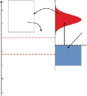
(a) Schematic diagram of plasmon-induced charge separation and associated photochemistry at the metal-
semiconductor heterojunction. (b) Optical simulations showing SPR-enhanced electric ields owing to photo-
excited Au particles, permeating into a neighboring TiO
2
structure. (a: Adapted with permission from Linic, S.,
Christopher, P., Ingram, D.B.
Nat. Mater.
, 10, 911. Copyright 2012, Nature Publishing Group. b: Adapted with per-
mission from Liu, Z., Hou, W., Pavaskar, P., Aykol, M., Cronin, S.B.
Nano Lett.
, 11, 1111. Copyright 2011, American
Chemical Society.)