Environmental Engineering Reference
In-Depth Information
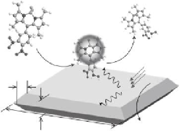
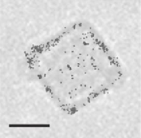
(a)
(b)
HN-BODIPY
highly fluorescent
UV light
DN-BODIPY
nonfluorescent
CH
3
OH
e
-
h
+
~0.5 µm
2 µm
~4 µm
~1 µm
Products
FIGURE 11.17
(See color insert.)
(a) Photocatalytic generation of luorescent HN-BODIPY from nonluorescent DN-BODIPY
over a TiO
2
crystal. (b) Transmission images of the same TiO
2
crystal immobilized on a cover glass in Ar-saturated
methanol solution containing DN-BODIPY under a 488-nm laser and UV irradiation. The blue and red dots in
the transmission image indicate the location of luorescence bursts on the {001} and {101} facets of the crystal,
respectively, observed during 3-min irradiation. (Adapted with permission from Tachikawa, T., Yamashita, S.,
Majima, T.,
J.
Am. Chem. Soc
., 133, 7197. Copyright 2011, American Chemical Society.)
electrons and holes toward speciic facets, which is presumably related to the facet-speciic
trapping sites and electronic energy levels (Figure 11.17).
71
Determining the relationship between the photocatalytic activity and crystal facets is
necessary for designing eficient photocatalysts by proper crystal facet engineering. A con-
ventional view is that the photoreactivity is proportional to the percentage of anatase TiO
2
{001} facets. However, there are conlicting experimental indings on the optimal ratio of
{001} facets to other exposed facets for photoreactivity. For instance, Pan et al. found that
the {001} facet exhibited a lower reactivity than the {101} facet in photocatalytic H
2
evolu-
tion.
61
Obviously, other surface states, including surface defects, surface chemistry, and the
substrate molecules, should be taken into account in explaining the function of {001} facets
on the photocatalytic reaction kinetics.
11.5 Conclusions and Perspectives
The semiconductor photocatalytic technology has been an increasing topic of interest
worldwide owing to its signiicance in environmental applications. From the semiconduc-
tor behavior upon excitation by photons to the utilization of photogenerated charge carri-
ers, nanotechnologies including energy band engineering and heterojunction structures
provide effective tools to improve photocatalytic activity. To realize a substantial break-
through in eficiency for photocatalytic settings, a better understanding of the charge
transfer processes across the surface/interface is greatly desired. Furthermore, a further
insight into the interactions between environmental contaminants and semiconductor
surface by
in situ
observation technologies is challenging but crucial for the optimiza-
tion of the photocatalytic reactions. Environment remediation will continue to serve as
an important platform to establish fundamental depth in photocatalysis, thus guiding the
future design, fabrication, and modiication of photocatalytic materials.