Image Processing Reference
In-Depth Information
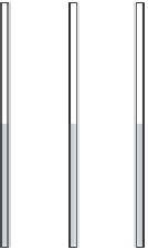
31
32
33
Image area
Image area
21
22
23
11
12
13
Storage area
Storage area
31
32
33
Output signal
21
22
23
S11
11
12
13
HCCD
(a)
Output part
(d)
Output part
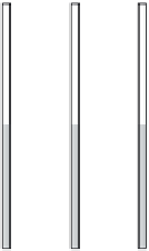
Image area
Image area
31
32
33
Storage area
Storage area
21
22
23
Output signal
31
32
33
11
12
13
S11,S12,S13
21
22
23
HCCD
(b)
Output part
(e)
Output part
31
32
33
Image area
Image area
21
22
23
11
12
13
Storage area
Storage area
31
32
33
Output signal
21
22
23
S31,S32,S33
S21,S22,S23
S11,S12,S13
11
12
13
HCCD
(c)
(f)
Output part
Output part
FIGURE 5.28
(a-f) Schematic diagram of FT-CCD operation.
between the image area and horizontal shift register (HCCD) of an IT-CCD, as shown in
Fig u re 5.29.
The operation to read out signal charges integrated in PDs to the VCCD is the same as
in IT-CCDs. Frameshift, in which charges in the VCCD are transferred to the storage area
at high frequency, follows the same as in FT-CCDs. Charge packets in the storage area are
transferred to the HCCD line by line, and transferred charge packets are converted to volt-
age signal output at the output amplifier one by one, in the same manner as in IT-CCDs
and FT-CCDs. The major purpose of this type of sensor is to achieve a very low smear
level. By high-speed frameshift, charge packets pass through the image area being irradi-
ated in a short time. This reduces the time factor of smear phenomenon. While the vertical