Image Processing Reference
In-Depth Information
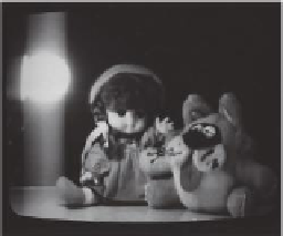
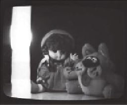
(a)
(b)
(c)
FIGURE 5.15
Images at high-intensity light irradiation: (a) blooming phenomenon; (b) blooming suppression, low smear sup-
pression; (c) blooming and smear suppression.
Figure 5.16 is a schematic diagram of the mechanism of the blooming phenomenon. In
practical use, this kind of image collapse has to be avoided. The means for excess charges
to discharge is an overflow drain. The first to be proposed is a lateral overflow drain,
10
shown in Figure 5.17. An overflow control gate and overflow drain are formed adjacent to
the PD. The channel potential under the overflow control gate is controlled so that excess
charges flow to the overflow drain before spilling over to the VCCD channel. Thus, a lat-
eral overflow drain and overflow control gate can suppress blooming and images such
as Figure 5.15b are obtained. However, they waste the active area of the silicon surface,
because they do not contribute to performance such as sensitivity or dynamic range. They
decrease the available area for the PD and VCCD, that is, performance decrement. And
that is where the VOD structure is.
11
PD
HCCD
Output amplifier
VCCD
PD
FIGURE 5.16
Mechanism of blooming.