Image Processing Reference
In-Depth Information
32
31
33
31
32
33
21
22
23
(a)
(e)
21
22
23
12
11
13
Output signal
HCCD
S11,S12,S13
HCCD
Output part
Output part
31
33
32
22
(b)
21
23
(f)
12
13
31
32
33
11
Output signal
HCCD
S11,S12,S13
21
22
23
Output part
Output part
(c)
(g)
31
32
33
21
21
22
22
23
23
Output signal
S21,S22,S23
S11,S12,S13
31
32
33
11
12
13
Output part
Output part
31
31
32
33
33
(d)
31
32
33
(h)
22
23
21
Output signal
21
22
23
11
12
13
S31,S32,S33
Output signal
S21,S22,S23
S11,S12,S13
S11
13
11
12
HCCD
HCCD
Output part
Output part
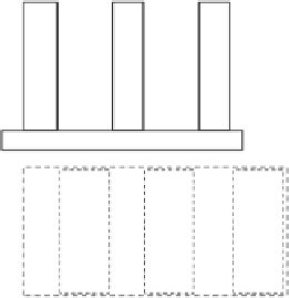
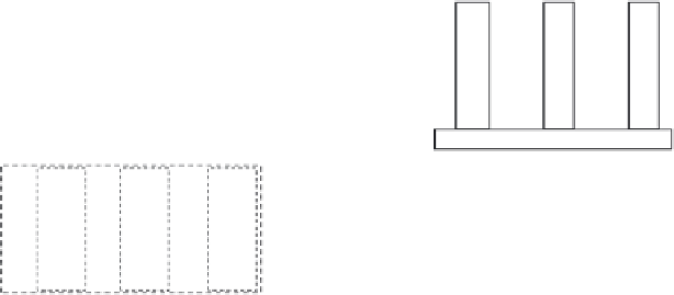
FIGURE 5.9
(a-h) Schematic diagram of IT-CCD operation in progressive mode.
5.1.1.2 Basic Pixel Structure of IT-CCD
A representative pixel structure of IT-CCD is shown as a 3D-like illustration in Figure 5.10.
A channel of a BCCD and a pinned PD are formed in the
p
-well built in the
n
-type sub-
strate. The
n
-type region of PD is basically surrounded by a
p
-type region, including two
sides of separation between neighboring PDs, although they are not shown explicitly in the
figure. The surface side of the PD is covered with a
p
+
layer to construct a pinned PD. Since
the PD receives incident light, no material that decreases light intensity by absorption or
reflection is formed above the PD. On the VCCD channel, two polysilicon transfer gates,
ϕV4 and ϕV1, are formed on contact with a gate-insulating layer such as SiO
2
. Figure 5.10
shows a representative pixel configuration with two transfer electrodes per pixel. A pixel
with two transfer electrodes of ϕV2 and ϕV3 is put on the near side in the transfer direc-
tion next to the pixel of the figure, and the two types of pixel are arrayed alternately to
form a four-phase CCD. Zero (GND) and positive V-sub biases are applied to
p
-well and
n
-type substrates, respectively. As will be discussed in Section 5.1.2.1, V-sub voltage is set
so that excess carriers generated in PDs overflow to the
n
-substrate before they spill over
to the VCCD channel or neighboring PDs. Here, gate electrode ϕV1, which is one polysili-
con layer, plays the roles of not only a transfer electrode in the VCCD but also a transfer
electrode to read out signal charges in PDs to the VCCD channel. Therefore, the electrode
is extended to the area above the charge readout path in the figure. Clock pulses applied
to electrodes are shown in Figure 5.11 for the interlaced mode. In this case, three-value