Image Processing Reference
In-Depth Information
V
d
Reset tr.
Signal charges
Potential of capacitor
C
(principle of charge-voltage conversion)
Q
Amplifier
Q
Signal voltage
V
Q
=
Q
/
C
φ
S
φ
B
C
V
d
(a)
(b)
(c)
Easily obtainable higher signal
voltage with lower capacitance
Signal
voltage
Signal
voltage
V
d
C
1
>
C
2
(d)
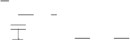
FIGURE 2.23
Working principle of FDA: (a) configuration; (b) electric potential of the capacitance just after reset operation;
(c) electric potential of the capacitance after reception of signal charges; (d) capacity and signal voltage.
capacitor
C
becomes lower, the higher signal voltage is easily obtained and this is advanta-
geous for the later signal processing from the viewpoint of signal-to-noise ratio.
On the other hand, if the capacitor volume is too low, the maximum charge amount in this
capacitor is limited because of the saturation under the treatable voltage range. And if a high
voltage range is adopted, the output will be out of the voltage range at a later stage. As these
conditions sometimes limit the saturation characteristics, a balanced design is required.
Since this capacitor becomes electrically isolated to be floating after being reset to sense the
potential change by the introduction of the signal charges, it is called floating diffusion (FD).
In the circuit of Figure 2.23a, the amplifier that is commonly used to sense the potential
of capacitor
C
is a source follower amplifier (SFA), which is discussed next.
2.3.2 Source Follower Amplifier
A source follower amplifier (SFA) is a so-called
buffer circuit
, which accepts the input signal
potential at the gate input part with high input impedance of MOSFET and produces the
same potential of output with low output impedance. Other circuits for the same kinds of
purposes are emitter follower circuits, which use bipolar transistors, and voltage follower
circuits, which use operational amplifiers. SFAs accept the input voltage
V
in
at the gate
input part and produce the output voltage
V
out
at the source output part.
As Figure 2.24a shows, the drive transistor (MOSFET) with the voltage input part and
load devices are connected in series in SFAs. Load devices include elements such as a
constant current source, shown in Figure 2.24b, a resistor, shown in Figure 2.24c, and a
load transistor, shown in Figure 2.24d. Each voltage-current characteristic of the drive