Image Processing Reference
In-Depth Information
Light
Signal charge
Silicon surface
Conduction band
Wholly depleted region
Interface
state
p
+
SiO
2
n
p
Light
Wholly
depleted
region
Electron-hole
pair generation
Valence band
n
-type
p
-type
p
+
-type
(a)
(b)
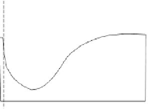
FIGURE 2.18
Buried/pinned photodiode: (a) cross-sectional view; (b) operation in energy space.
2.2 Silicon as a Photosensitive Material
Silicon is a key material of LSI circuits, and image sensors are LSI circuits. Also, silicon
absorbs light of ultraviolet, visible, and near-infrared wavelength regions to generate
charge. Therefore it is natural that silicon has come to be used in photosensitive parts in
image sensors. However, this does not mean that silicon is the best photosensitive material
for all image sensors.
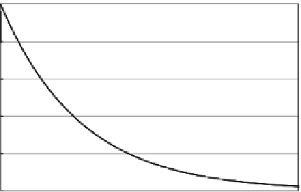
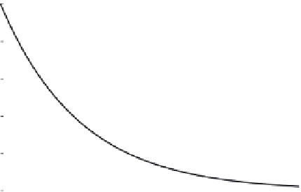
As Figure 2.19 shows, the luminous flux density ϕ travels through silicon being absorbed.
The luminous flux density reduces the amount of Δϕ while advancing the distance of Δ
x
because of absorption. Expressing absorption coefficient α, the relationship is shown as
follows:
∆
φ
=−
φ
∆
x
(2.3)
1
0.8
Gradient: -
α
∆ φ
∆ φ =
-
α φ ∆
x
∆
x
0.6
α
: Absorption coe
cient
0.4
1/
e
0.2
0
Surface
d
λ
Depth
x
→
FIGURE 2.19
Depth dependence of luminous flux density.