Image Processing Reference
In-Depth Information
Quadratic functionofdepth
x
Inside apart
from interface
Depleted region
Conduction band
V
G
= 0 V
p
-type
n
-type
Valence band
x
Interface
: Electron
: Ionized donor
: Hole
: Ionized acceptor
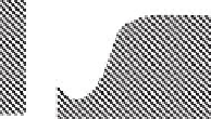
FIGURE 2.15
Schematic potential profile of buried MOS structure.
2.1.5 Photogate
Photosensitive element components are now described. The characteristics of silicon as
a photosensitive material will be explained in Section 2.2. It is assumed that the signal
charge is an electron unless otherwise noted.
Photogate sensors are MOS structures, as shown in Figure 2.16a. The application of
positive voltage to the gate electrode forms a depletion layer with the maximum poten-
tial at the surface, as shown in Figure 2.16b. The light transmitted through the gate
electrode is absorbed in silicon and generates a pair of an electron and a hole. The
electric field in a depletion layer separates them spatially. Electron-hole pairs created in
deeper positions in substrate where there is no electric field tend to vanish by recombi-
nation because there is no force to separate them, shown as generation and recombina-
tion in Figure 2.16b. The electrons are collected in the potential well at the surface, and
the holes move to the substrate side to be discharged finally outside the device. Here
the gate electrode must allow light to pass through, so metals cannot be used as the
Light-permeable gate electrode (polysilicon, etc.)
Light
+
V
G
Conduction band
Signal charge
Generation
Recombination
Generation
SiO
2
Light
Valence band
Depletion
layer
p
-type Si
Electron-hole pair
generation
p
-type silicon
(a)
(b)
FIGURE 2.16
Photogate: (a) cross-sectional view; (b) operation in energy space.