Image Processing Reference
In-Depth Information
n
-
n
-
SiO
2
(a)
(c)
p
-type Si
p
-type Si
-
-
-
+
-
-
-
+
-
p
-
+
+
+
+
+
+
+
+
p
+
+
V
G
-
-
-
-
-
-
-
-
-
-
-
-
-
-
-
V
G
+ + +
+++
+++
+++
+
+
+
+
+
+
-
-
-
-
--
-
Depletion layer
Depletion layer
By removing electrons
What shape of potential profile
is formed?
(b)
(d)
Conduction band
Conduction band
V
G
= 0 V
p
-type
V
G
= 0 V
p
-type
n
-
Valence
band
Valence
band
-
: Electron
: Hole
+
: Ionized donor
: Ionized acceptor
+
-
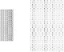
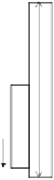
FIGURE 2.13
Charge and potential distribution of buried MOS structure: (a) spatial distribution (not depleted); (b) potential
distribution (not depleted); (c) spatial distribution (fully depleted); (d) potential distribution (fully depleted).
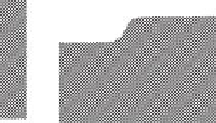
positive voltage, the
n
-type area will be completely depleted and only positively charged
ionized donors spatially fixed will be distributed, as indicated in Figure 2.13c. How is the
potential distribution in the
n
-type layer indicated in Figure 2.13d?
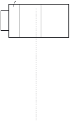
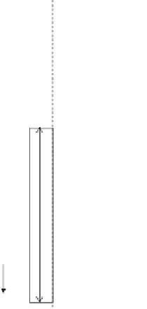
Here, a very simplified way to consider this situation is introduced, as shown in
Figure 2.14a.
1
1. The spatial distribution of positive charges (ionized donors) is uniform.
2. Both sides of the
n
-type layer are grounded, that is, the potential profile is bilater-
ally symmetric, including the boundary conditions.
The electric potential ϕ of this area is expressed by the Poisson equation as follows:
2
d
d
φρ
κε
−
(
)
=
constant
2
x
0
(2.1)
ρ=
eN
D
where
x
is depth
ρ = charge density
κ = relative permittivity of silicon