Image Processing Reference
In-Depth Information
Pixel conversion (6.85 µs)
φ
S
φ
RST
φ
TX
2.3 µs = 110 cycles
2.3 µs = 110 cycles
pixel
Reset conversion
Signal conversion
φ
RT
φ
R2
φ
BW1
Decimation
filter weight
Modulator
output
Digital CDS
D
O
=
D
SIG
-
D
RST
Second-order function
Second-order function
Decimation filter
output
D
RST
D
O
D
SIG
Bit-wise inversion
D
RST
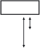
FIGURE 5.64
Timing diagram of one horizontal conversion. (Reprinted with permission from Chae, Y., Cheon, J., Lim, S.,
Kwon, M., Yoo, K., Jung, W., Lee, D., Ham, S., and Han, G.,
Journal of Solid State Circuits
, 46, 236-247, 2011.)
5.3.3.2.3 Pixel-Level ADC Sensor
If A/D conversion of light intensity information is done in the pixel, no new noise is added
through the readout pass. This is not only a great advantage in terms of SNR, but also a
very important functionality because of flexible operation or signal processing at intra- and
interpixel levels. As processing is at each pixel level, it is the ultimate parallel treatment
and also benefits high-speed performance. Depending on the method and application,
the frame-based accumulation mode, which almost all image sensors adopt, might not be
necessary. It is highly expected that flexibility and high functionality in the time domain
will be improved spectacularly.
While there are examples of all kinds of ways to develop pixel-level ADC sensors
through the front door, a unique sensor is introduced here. Although this sensor is usu-
ally categorized as a wide dynamic range sensor, it can be considered as a pixel-level ADC
sensor. But no so-called “A/D converter” circuit is used. This sensor is the first example
that does not belong to “almost all image sensors” in this topic, as described in the irst
footnote in Section 1.2.3. The pixel circuit diagram and output of pulse photosensor
51
are
shown in Figure 5.65a and b, respectively.