Image Processing Reference
In-Depth Information
Column amplifier
Successive approximate ADC
Dual comparator
Pixel output
φ
SH
-
-
-
+
V
ref
+
+
DAC
MSB
LSB
V
BIAS
2
13-4
C
0
2
12-4
C
0
2
m-2
C
0
2
0
C
0
Latch
Latch
Latch
V
ref
1⁄ 2
2
V
ref
1 ⁄ 2
4
V
ref
1
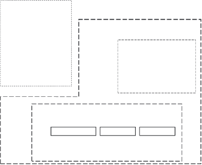
FIGURE 5.59
Circuit diagram of a 14-bit successive-approximation ADC. (Adapted from Matsuo, S., Bales, T.J., Shoda, M.,
Osawa, S., Kawamura, K., Andersson, A., Haque, M., et al.,
Transactions on Electron Devices
, 56(11), 2380-2389,
2009. With permission.)
Figure 5.60 is a block diagram of a cyclic-type ADC sensor.
47
Although circuit configura-
tions were complicated in origin, an architecture applicable to image sensors was proposed.
48
A circuit configuration of a 13-bit cyclic column-parallel ADC is shown in Figure 5.61.
This ADC is made up of an operational transconductance amplifier (OTA), capacitance
(
C
1
=
C
,
C
2
=
C
/2), sub-ADC composed of two comparators, and DAC. Before A/D conver-
sion, the system is initialized by setting all the switches on-state to reset all charges remain-
ing in the capacitances. This operation enables high-precision digital CDS. During sampling,
inputs are applied to the sub-ADC to determine the most significant bit, and the sub-ADC
compares
V
IN
with two reference voltages (
V
RCH
,
V
RCL
) and generates three kinds of digital
code
D
([
D
1
,
D
0
]), whose values are 0, 1, or 2. Switches in the DAC are controlled by using
the digit of the most significant bit. As capacitances (
C
1a
and
C
2b
) that are connected to the
inverting input terminal of the amplifier are connected with
V
RCH
or
V
RCL
, the input
V
IN
is
multiplied by two and a reference level is subtracted from it. Then, amplifier output is sam-
pled by capacitances
C
1a
and
C
1b
and fed back for the second significant bit determination.
Multiplications and feedbacks are repeated until the necessary digit codes are obtained. To
obtain 13 bits, they are repeated 11 times. This sensor has 5.6 μm pitch and 300 k pixels with
very-low-level column FPN of 0.1 electrons and a high frame rate of 390 fps.
5.3.3.2.2.4
ΔΣ
-Type ADC
Figure 5.62 is a block diagram of an ADC sensor
49, 50
developed
for realization of low noise and wide dynamic range by using a ΔΣ ADC with a narrow
circuit area and low power consumption. It is generally known that ΔΣ ADCs achieve high