Hardware Reference
In-Depth Information
The Control register at address 0x07 determines how the SQW/OUT pin behaves.
When
SQWE=1
, a square wave signal is produced at the SQW/OUT pin. The frequency is
selected by bits
RS1
and
RS0
. In this mode, the
OUT
setting is ignored.
When
SQWE=0
, the
SQW/OUT
pin is set according to the bit placed in
OUT
(bit 7 of the
control register). In this mode, the pin behaves as an open-drain GPIO output pin.
Reading Date and Time
When the DS1307 device is being read, a snapshot of the current date and time is made
when the I2C start bit is seen. This copy operation allows the clock to continue to run
while returning a stable date/time value back to the master. If this were not done, time
components could change between reading bytes. The application should therefore
always read the full date/time set of registers as one I/O operation. The running clock
does not affect reading the control register or the RAM locations.
I2C Communication
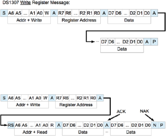
The DS1307 registers and RAM can be written randomly, by specifying an initial starting
register address, followed by 1 or more bytes to be written. The register address is
automatically incremented with each byte written and wraps around to 0. The DS1307
slave device will ACK each byte as it is received, continuing until the master writes a stop
bit (P). The first byte sent is always the peripheral's I2C address, which should not be
confused with the selected peripheral's register address (that immediately follows). The
DS1307 I2C address is always 0x68. The general form of the write message is shown here:
The DS1307 supports multibyte reads. You can read multiple bytes from the DS1307
simply by starting with an I2C start bit (S), and peripheral address sent as a read request.
The slave will then serve up bytes one after another for the master. Receiving terminates
when the master sends a NAK.