Hardware Reference
In-Depth Information
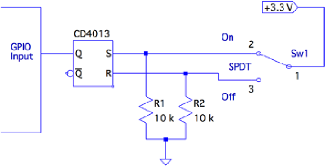
Figure 8-1.
Using a flip-flop for debouncing
When the switch is releasing one contact, there is no change in the flip-flop output.
After the arm has flown through its switching arc, the opposite contact eventually starts
to bounce at the end of its swing. At this point, it takes only a single pulse to change the
output of the flip-flop to its new state. After that, it remains constant.
The pull-down resistors
R
1
and
R
2
are necessary because the CMOS inputs would
otherwise float when the switch arm disconnects from the switch's contacts. While
disconnected, the resistors pull the input voltage down to ground potential.
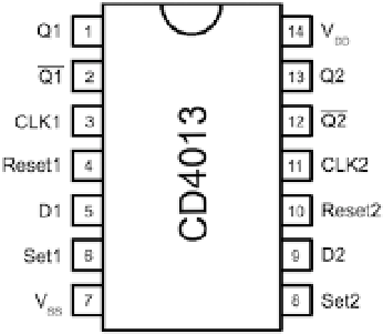
The CD4013
The CD4013 is a CMOS part that is able to operate from +3 V and up. The pinout for the
CD4013 is provided in Figure
8-2
. The supply voltage
V
DD
is applied to pin 14, with pin 7
(
V
SS
) performing as the ground return. From the pinout diagram, you can see that this is a
dual flip-flop IC, with pins labeled for units 1 and 2.
Figure 8-2.
The CD4013 pinout