Hardware Reference
In-Depth Information
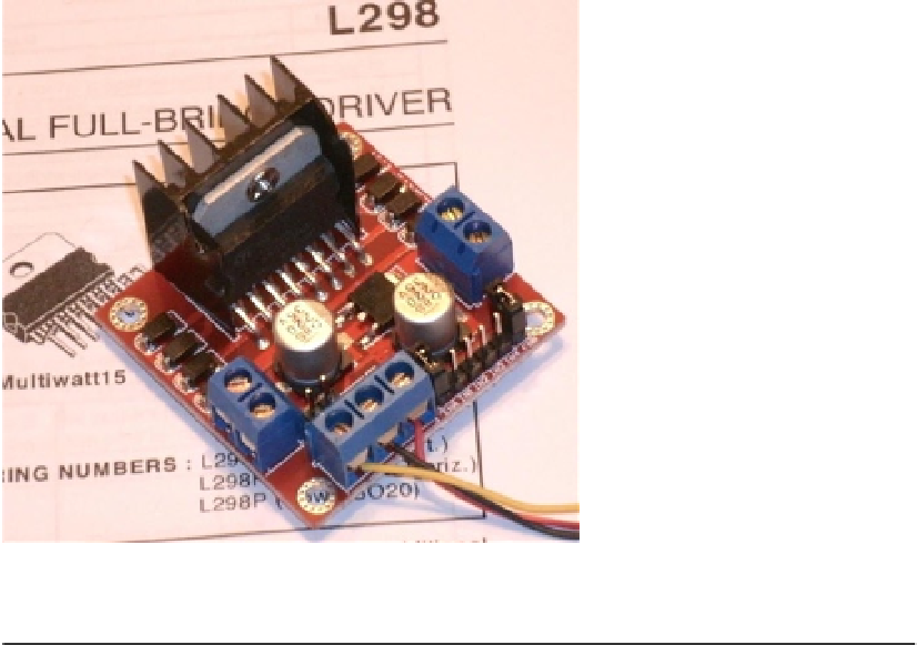
Figure 7-3.
L298 driver PCB
■
Note
i purchased this pCB as an eBay Buy it Now offer with free shipping.
The PCB has three power connections:
•
V
S
, which is labeled as +12 V (yellow wire in the photo)
Gnd (black wire)
•
•
V
SS
, which is labeled as +5 V (red wire)
This particular PCB has a jumper (removed in Figure
7-3
), with its two pins visible
just above the power-connection block and below the round capacitor. With the jumper
installed, an onboard regulator supplies
V
SS
with +5 V from the
V
S
(+12 V) input. The
regulated +5 V is also available for external circuitry at the block connector (where the red
wire is shown).
When the motor (
V
S
) voltage is higher than 12 V, it is best to remove the jumper and
supply the +5 V into the block instead. The reason for this is that the linear regulator must
dissipate additional heat from the higher input voltage. I am using a salvaged power
supply with both a +5 V supply and a +16 V supply, so the jumper was removed.
To the right of the power-input block are header connection pins as follows:
+5V
+5V
EnA
In1
In2
In3
In4
EnB